SSM6G18NU
SSM6G18NU is Silicon Epitaxial Schottky Barrier Diode manufactured by Toshiba.
posite Devices Silicon P-Channel MOS / Epitaxial Schottky Barrier
1. Applications
- Power Management Switches
2. Features
(1) bined a P-channel MOSFET and a Schottky barrier diode in one package.
2.1. MOSFET Features
(1) Low drain-source on-resistance : RDS(ON) = 261 mΩ (max) (VGS = -1.5 V) RDS(ON) = 185 mΩ (max) (VGS = -1.8 V) RDS(ON) = 143 mΩ (max) (VGS = -2.5 V) RDS(ON) = 112 mΩ (max) (VGS = -4.5 V)
2.2. Diode Features
(1) Low forward voltage: VF = 0.48 V (typ.) (@IF = 1000 mA)
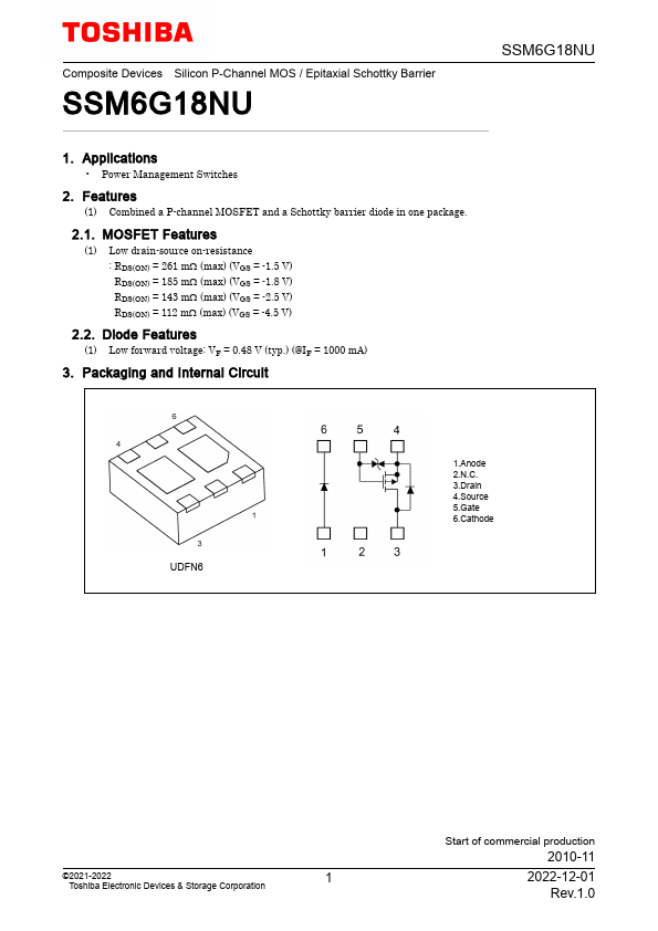
3. Packaging and Internal Circuit
UDFN6
1.Anode 2.N.C. 3.Drain 4.Source 5.Gate 6.Cathode
©2021-2022
Toshiba Electronic Devices & Storage Corporation
Start of mercial...