SSM6J06FU
SSM6J06FU is Power Management Switch manufactured by Toshiba.
TOSHIBA Field Effect Transistor Silicon P Channel MOS Type
Power Management Switch High Speed Switching Applications
- -
- Small package Low on resistance : Ron = 0.5 Ω max (VGS =
- 4 V) : Ron = 0.7 Ω max (VGS =
- 2.5 V) Low gate threshold voltage
..
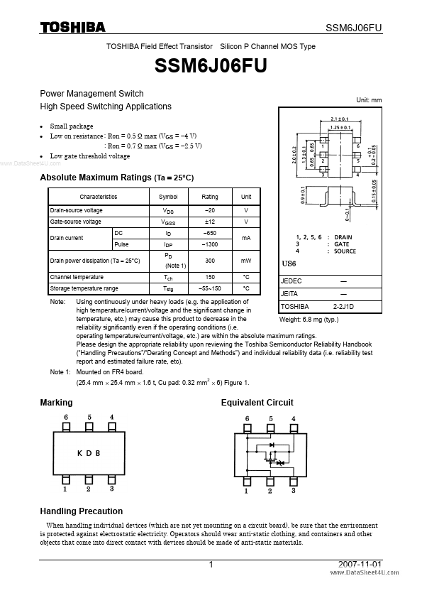
Unit:...