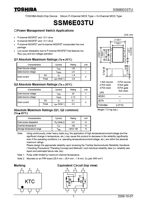
low RDS (ON) and low-voltage operation
1 2 3
6 5 4
Q1 Absolute Maximum Ratings (Ta = 25°C)
Characteristics Drain-Source voltage Gate-Source voltage Drain current DC Pulse Symbol VDS VGSS ID IDP (Note 1) Rating.
20 ±8 -1.8 -3.6 Unit
V V
A
0.7±0.05
Q2 Absolute Maximum Ratings (Ta = 25°C)
Characteristics Drain-Source voltage Gate-Source voltage Drain current DC Pulse Symbol VDS VGSS ID IDP (Note 1) Rating 20 ± 10 0.1 0.2 Unit V V A
1.Nch source 2.Pch drain 3.Pch drain UF6 JEDEC JEITA.
Full PDF Text Transcription for SSM6E03TU (Reference)
Note: Below is a high-fidelity text extraction (approx. 800 characters) for
SSM6E03TU. For precise diagrams, and layout, please refer to the original PDF.
SSM6E03TU TOSHIBA Multi-Chip Device Silicon P-Channel MOS Type + N-Channel MOS Type SSM6E03TU Power Management Switch Applications • • • • Unit: mm P-channel MOSFET and 1...
View more extracted text
Management Switch Applications • • • • Unit: mm P-channel MOSFET and 1.8 V drive N-channel MOSFET and 1.5 V drive P-channel MOSFET and N-channel MOSFET incorporated into one package. 0.65 0.65 2.0±0.1 1.3±0.1 2.1±0.1 1.7±0.1 +0.1 0.3-0.05 Low power dissipation due to P-channel MOSFET that features low RDS (ON) and low-voltage operation 1 2 3 6 5 4 Q1 Absolute Maximum Ratings (Ta = 25°C) Characteristics Drain-Source voltage Gate-Source voltage Drain current DC Pulse Symbol VDS VGSS ID IDP (Note 1) Rating −20 ±8 -1.8 -3.6 Unit V V A 0.7±0.