V20120SG-E3, VF20120SG-E3, VB20120SG-E3, VI20120SG-E3
www.vishay.com
Vishay General Semiconductor
High Voltage Trench MOS Barrier Schottky Rectifier
Ultra Low VF = 0.54 V at IF = 5 A
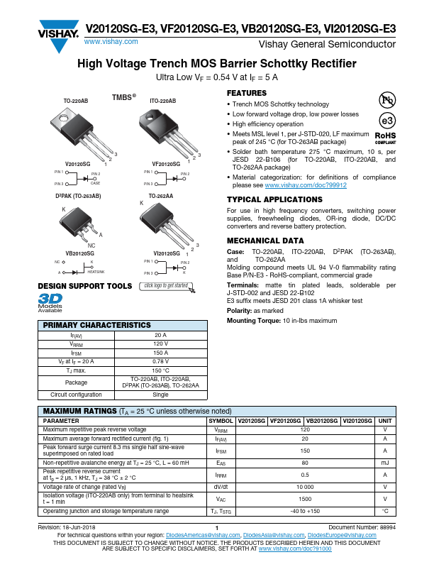
TO-220AB
TMBS ®
ITO-220AB
V20120SG
3
2
1
PIN 1
PIN 2
PIN 3
CASE
D2PAK (TO-263AB)
K
VF20120SG 1 2 3
PIN 1
PIN 2
PIN 3
TO-262AA
K
A
NC
VB20120SG
NC K
A HEATSINK
DESIGN SUPPORT TOOLS
3
2
VI20120SG 1
PIN 1
PIN 2
PIN 3
K
click logo to get started
Models
Available
PRIMARY CHARACTERISTICS
IF(AV)
VRRM
IFSM
VF at IF = 20 A
TJ max.
Package
20 A
120 V
150 A
0.78 V
150 °C
TO-220AB, ITO-220AB,
D2PAK (TO-263AB), TO-262AA
Circuit configuration
Single
FEATURES
• Trench MOS Schottky technology
• Low forward voltage drop, low power losses
• High efficiency operation
• Meets MSL level 1, per J-STD-020, LF maximum
peak of 245 °C (for TO-263AB package)
• Solder bath temperature 275 °C maximum, 10 s, per
JESD 22-B106 (for TO-220AB, ITO-220AB, and
TO-262AA package)
• Material categorization: for definitions of compliance
please see www.vishay.com/doc?99912
TYPICAL APPLICATIONS
For use in high frequency converters, switching power
supplies, freewheeling diodes, OR-ing diode, DC/DC
converters and reverse battery protection.
MECHANICAL DATA
Case: TO-220AB, ITO-220AB, D2PAK (TO-263AB),
and TO-262AA
Molding compound meets UL 94 V-0 flammability rating
Base P/N-E3 - RoHS-compliant, commercial grade
Terminals: matte tin plated leads, solderable per
J-STD-002 and JESD 22-B102
E3 suffix meets JESD 201 class 1A whisker test
Polarity: as marked
Mounting Torque: 10 in-lbs maximum
MAXIMUM RATINGS (TA = 25 °C unless otherwise noted)
PARAMETER
SYMBOL V20120SG VF20120SG VB20120SG
Maximum repetitive peak reverse voltage
Maximum average forward rectified current (fig. 1)
Peak forward surge current 8.3 ms single half sine-wave
superimposed on rated load
VRRM
IF(AV)
IFSM
120
20
150
Non-repetitive avalanche energy at TJ = 25 °C, L = 60 mH
Peak repetitive reverse current
at tp = 2 μs, 1 kHz, TJ = 38 °C ± 2 °C
Voltage rate of change (rated VR)
Isolation voltage (ITO-220AB only) from terminal to heatsink
t = 1 min
EAS
IRRM
dV/dt
VAC
80
0.5
10 000
1500
Operating junction and storage temperature range
TJ, TSTG
-40 to +150
VI20120SG
UNIT
V
A
A
mJ
A
V
V
°C
Revision: 18-Jun-2018
1 Document Number: 88994
For technical questions within your region: DiodesAmericas@vishay.com, DiodesAsia@vishay.com, DiodesEurope@vishay.com
THIS DOCUMENT IS SUBJECT TO CHANGE WITHOUT NOTICE. THE PRODUCTS DESCRIBED HEREIN AND THIS DOCUMENT
ARE SUBJECT TO SPECIFIC DISCLAIMERS, SET FORTH AT www.vishay.com/doc?91000