Datasheet Summary
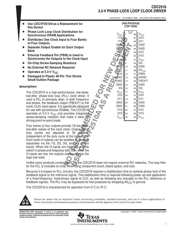
CDC2516 3.3ĆV PHASEĆLOCK LOOP CLOCK DRIVER
ą
SCAS579C
- OCTOBER 1996
- REVISED DECEMBER 2004
D Use CDCVF2510A as a Replacement for this Device
D Phase-Lock Loop Clock Distribution for
Synchronous DRAM Applications
D Distributes One Clock Input to Four Banks of Four Outputs
D Separate Output Enable for Each Output
Bank
D External Feedback Pin (FBIN) Is Used to
Synchronize the Outputs to the Clock Input
D On-Chip Series-Damping Resistors D No External RC Network Required D Operates at 3.3-V VCC D Packaged in Plastic 48-Pin Thin Shrink
Small-Outline Package description
The CDC2516 is a high-performance, low-skew, low-jitter, phase-lock loop (PLL) clock driver. It uses a PLL to precisely...