Datasheet Summary
D Low Output Skew for Clock-Distribution and Clock-Generation Applications
D TTL-patible Inputs and
CMOS-patible Outputs
D Distributes One Clock Input to Six Clock
Outputs
D Polarity Control Selects True or plementary Outputs
D Distributed VCC and GND Pins Reduce
Switching Noise
D High-Drive Outputs (- 32-mA IOH,
32-mA IOL)
D State-of-the-Art EPIC-ΙΙB™ BiCMOS Design
Significantly Reduces Power Dissipation
D Package Options Include Plastic
Small-Outline (D)
CDC329A 1-LINE TO 6-LINE CLOCK DRIVER
WITH SELECTABLE POLARITY
SCAS328B
- DECEMBER 1992
- REVISED OCTOBER 1998
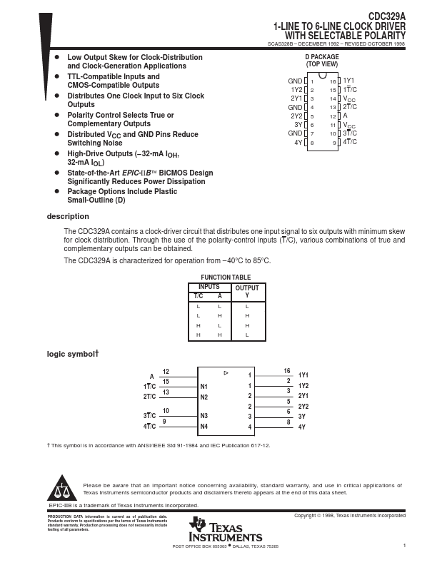
D PACKAGE (TOP VIEW)
GND 1 1Y2 2 2Y1 3 GND 4 2Y2 5
3Y 6 GND 7
4Y 8
16 1Y1 15 1T/C 14 VCC 13 2T/C 12 A 11 VCC 10...