Datasheet Summary
CDC857-2, CDC857-3 2.5-/3.3-V PHASE-LOCK LOOP CLOCK DRIVERS
SCAS627A
- SEPTEMBER 1999
- DECEMBER 1999
D Phase-Lock Loop Clock Distribution for
Double Data Rate Synchronous DRAM
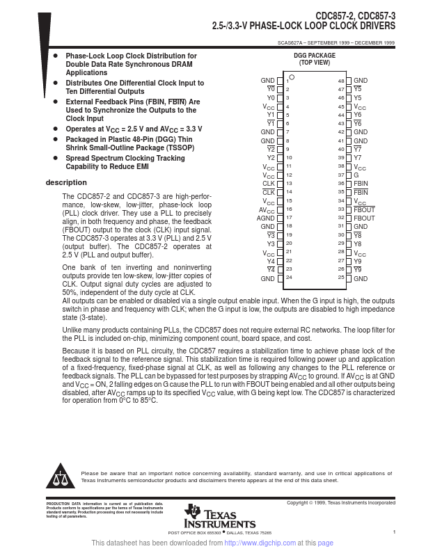
DGG PACKAGE (TOP VIEW)
Applications
D Distributes One Differential Clock Input to
Ten Differential Outputs
D External Feedback Pins (FBIN, FBIN) Are
Used to Synchronize the Outputs to the
Clock Input
D Operates at VCC = 2.5 V and AVCC = 3.3 V D Packaged in Plastic 48-Pin (DGG) Thin
Shrink Small-Outline Package (TSSOP)
D Spread Spectrum Clocking Tracking
GND 1 Y0 2 Y0 3
VCC 4 Y1 5 Y1 6
GND 7 GND 8
Y2 9 Y2 10
48 GND 47 Y5 46 Y5 45 VCC 44 Y6 43 Y6 42 GND 41 GND 40 Y7 39 Y7
Capability to Reduce EMI...