Datasheet Details
| Part number | CDC857-2 |
|---|---|
| Manufacturer | Texas Instruments |
| File Size | 155.46 KB |
| Description | 2.5-/3.3-V PHASE-LOCK LOOP CLOCK DRIVERS |
| Datasheet | CDC857-2-etcTI.pdf |
|
|
|
Overview: CDC857-2, CDC857-3 2.5-/3.3-V PHASE-LOCK LOOP CLOCK DRIVERS SCAS627A – SEPTEMBER 1999 – DECEMBER 1999 D Phase-Lock Loop Clock Distribution for Double Data Rate Synchronous DRAM DGG PACKAGE (TOP VIEW) Applications D Distributes One Differential Clock Input to Ten Differential Outputs D External Feedback Pins (FBIN, FBIN) Are Used to Synchronize the Outputs to the Clock Input D Operates at VCC = 2.5 V and AVCC = 3.
| Part number | CDC857-2 |
|---|---|
| Manufacturer | Texas Instruments |
| File Size | 155.46 KB |
| Description | 2.5-/3.3-V PHASE-LOCK LOOP CLOCK DRIVERS |
| Datasheet | CDC857-2-etcTI.pdf |
|
|
|
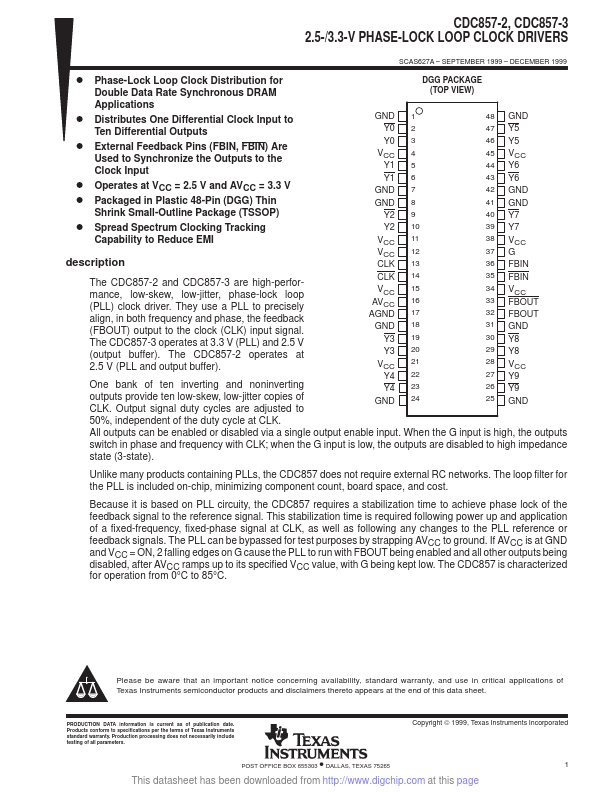
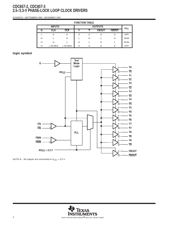
VCC 11 VCC 12 CLK 13 38 VCC 37 G 36 FBIN The CDC857-2 and CDC857-3 are high-performance, low-skew, low-jitter, phase-lock loop (PLL) clock driver.
They use a PLL to precisely align, in both frequency and phase, the feedback (FBOUT) output to the clock (CLK) input signal.
The CDC857-3 operates at 3.3 V (PLL) and 2.5 V (output buffer).
Compare CDC857-2 distributor prices and check real-time stock availability from major suppliers. Prices and inventory may vary by region and order quantity.
| Part Number | Description |
|---|---|
| CDC857-3 | 2.5-/3.3-V PHASE-LOCK LOOP CLOCK DRIVERS |
| CDC1104 | 1 to 4 Configurable Clock Buffer |
| CDC111 | 1-LINE TO 9-LINE DIFFERENTIAL LVPECL CLOCK DRIVER |
| CDC203 | 3.3-V HEX INVERTER/CLOCK DRIVER |
| CDC204 | HEX INVERTER/CLOCK DRIVER |
| CDC208 | Dual 1-Line To 4-Line Clock Drivers |
| CDC2351 | 1-LINE TO 10-LINE CLOCK DRIVER |
| CDC2351-EP | 1-Line to 10-Line Clock Driver |
| CDC2509B | 3.3-V Phase-Lock-Loop Clock Driver |
| CDC2509C | 3.3-V Phase-Lock-Loop Clock Driver |