Datasheet Summary
.ti.
SCAS684C
- SEPTEMBER 2002
- REVISED JANUARY 2008
Not Remended for New Designs
PROGRAMMABLE LOW-VOLTAGE 1:10 LVDS CLOCK DRIVER
Features
- Low-Output Skew <30 ps (Typical) for Clock-Distribution Applications
- Distributes One Differential Clock Input to 10 LVDS Differential Clock Outputs
- VCC range 2.5 V ±5%
- Typical Signaling Rate Capability of Up to
1.1 GHz
- Configurable Register (SI/CK) Individually Enables Disables Outputs, Selectable CLK0, CLK0 or CLK1, CLK1 Inputs
- Full Rail-to-Rail mon-Mode Input Range
- Receiver Input Threshold ±100 mV
- Available in 32-Pin LQFP Package
- Fail-Safe I/O-Pins for VDD = 0 V (Power Down)
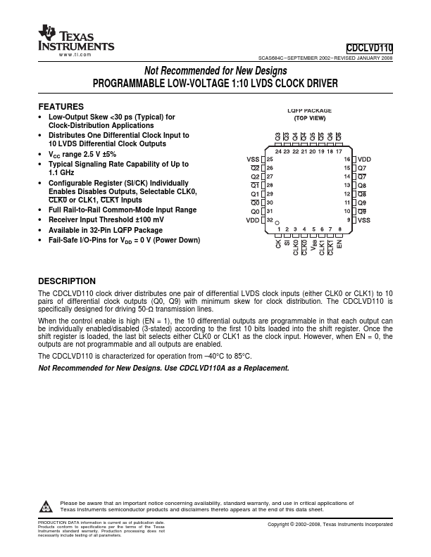
LQFP PACKAGE
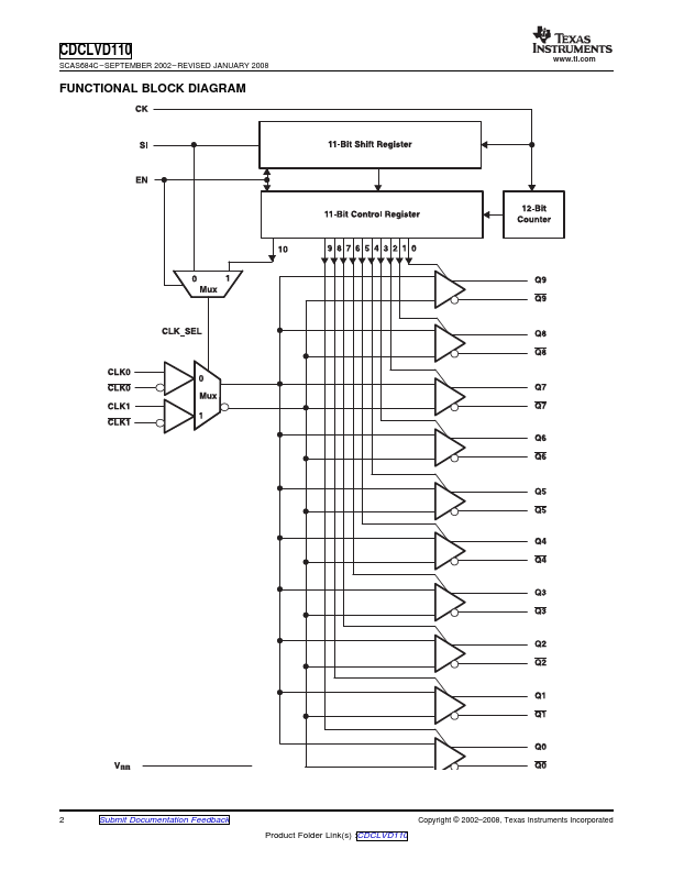
DESCRIPTION
The...