Datasheet Summary
Product Folder
Sample & Buy
Technical Documents
Tools & Software
Support & munity
SCAS841D
- FEBRUARY 2007
- REVISED DECEMBER 2016
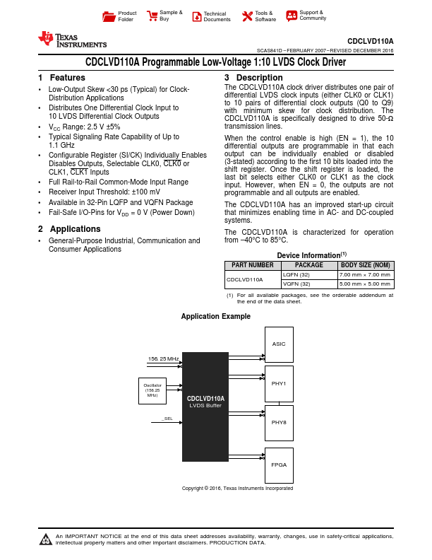
CDCLVD110A Programmable Low-Voltage 1:10 LVDS Clock Driver
1 Features
- 1 Low-Output Skew <30 ps (Typical) for ClockDistribution Applications
- Distributes One Differential Clock Input to 10 LVDS Differential Clock Outputs
- VCC Range: 2.5 V ±5%
- Typical Signaling Rate Capability of Up to
1.1 GHz
- Configurable Register (SI/CK) Individually Enables
Disables Outputs, Selectable CLK0, CLK0 or CLK1, CLK1 Inputs
- Full Rail-to-Rail mon-Mode Input Range
- Receiver Input Threshold: ±100 mV
- Available in 32-Pin LQFP and VQFN Package
- Fail-Safe...