DS99R421 Description
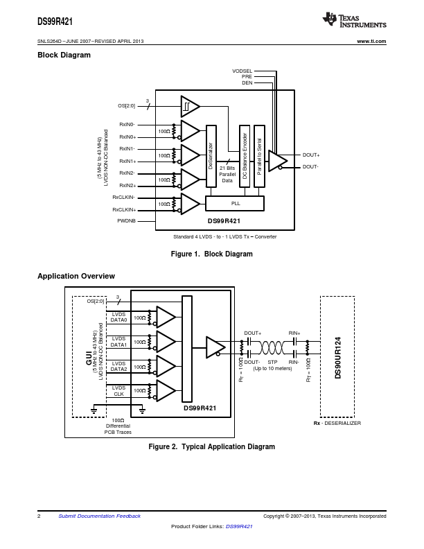
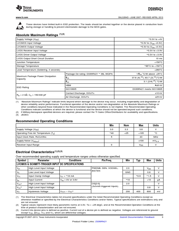
The DS99R421 converts a FPD-Link input with 4 non-DC Balanced LVDS (3 LVDS Data + LVDS Clock) plus 3 over-sampled low speed control bits into a single LVDS DC-balanced serial stream with embedded clock information. This single serial stream simplifies transferring the 24-bit bus over a single differential pair of PCB traces and cable by eliminating the skew problems between the 3 parallel LVDS data inputs and LVDS...
DS99R421 Key Features
- 2 5 MHz-43 MHz Embedded Clock & DCBalanced Data Transmission (21 Total LVDS Data Bits Plus 3 Low Speed LVCMOS Data Bits)
- User Adjustable Pre-Emphasis Driving Ability Through External Resistor on LVDS Outputs and Capable to Drive up to 10 Met
- Supports AC-Coupling Data Transmission
- 100Ω Integrated Termination Resistor at LVDS Input
- Power-Down Control
- Available @SPEED BIST to DS90UR124 to Validate Link Integrity
- All LVCMOS Inputs & Control Pins Have Internal Pulldown
- Schmitt Trigger Inputs on OS[2:0] to Minimize Metastable Conditions
- Outputs Tri-Stated Through DEN
- On-Chip Filters for PLLs