74HC74; 74HCT74
Dual D-type flip-flop with set and reset; positive edge-trigger
Rev. 6 — 21 April 2020
Product data sheet
1. General description
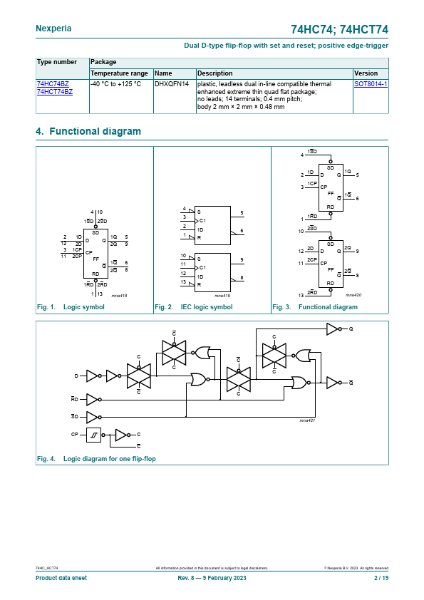
The 74HC74 and 74HCT74 are dual positive edge triggered D-type flip-flop. They have individual
data (nD), clock (nCP), set (nSD) and reset (nRD) inputs, and complementary nQ and nQ outputs.
Data at the nD-input, that meets the set-up and hold time requirements on the LOW-to-HIGH clock
transition, is stored in the flip-flop and appears at the nQ output. Schmitt-trigger action in the clock
input, makes the circuit highly tolerant to slower clock rise and fall times. Inputs include clamp
diodes that enable the use of current limiting resistors to interface inputs to voltages in excess of
VCC.
2. Features and benefits
• Input levels:
• For 74HC74: CMOS level
• For 74HCT74: TTL level
• Symmetrical output impedance
• Low power dissipation
• High noise immunity
• Balanced propagation delays
• Specified in compliance with JEDEC standard no. 7A
• ESD protection:
• HBM JESD22-A114F exceeds 2000 V
• MM JESD22-A115-A exceeds 200 V
• Multiple package options
• Specified from -40 °C to +85 °C and from -40 °C to +125 °C
3. Ordering information
Table 1. Ordering information
Type number Package
Temperature range Name
74HC74D
-40 °C to +125 °C SO14
74HCT74D
74HC74DB
-40 °C to +125 °C SSOP14
74HCT74DB
74HC74PW
-40 °C to +125 °C TSSOP14
74HCT74PW
74HC74BQ
-40 °C to +125 °C DHVQFN14
74HCT74BQ
Description
plastic small outline package; 14 leads;
body width 3.9 mm
plastic shrink small outline package; 14 leads;
body width 5.3 mm
plastic thin shrink small outline package; 14 leads;
body width 4.4 mm
plastic dual in-line compatible thermal enhanced
very thin quad flat package; no leads; 14 terminals;
body 2.5 × 3 × 0.85 mm
Version
SOT108-1
SOT337-1
SOT402-1
SOT762-1