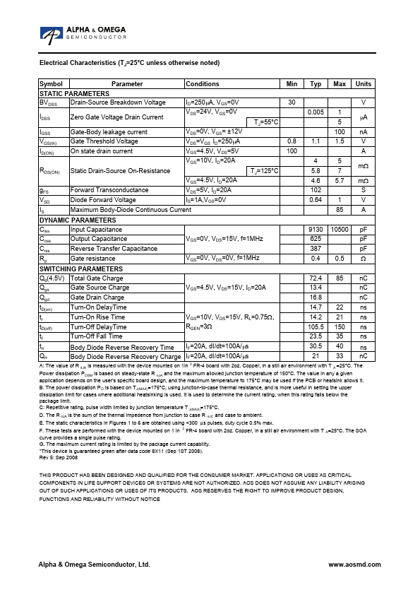
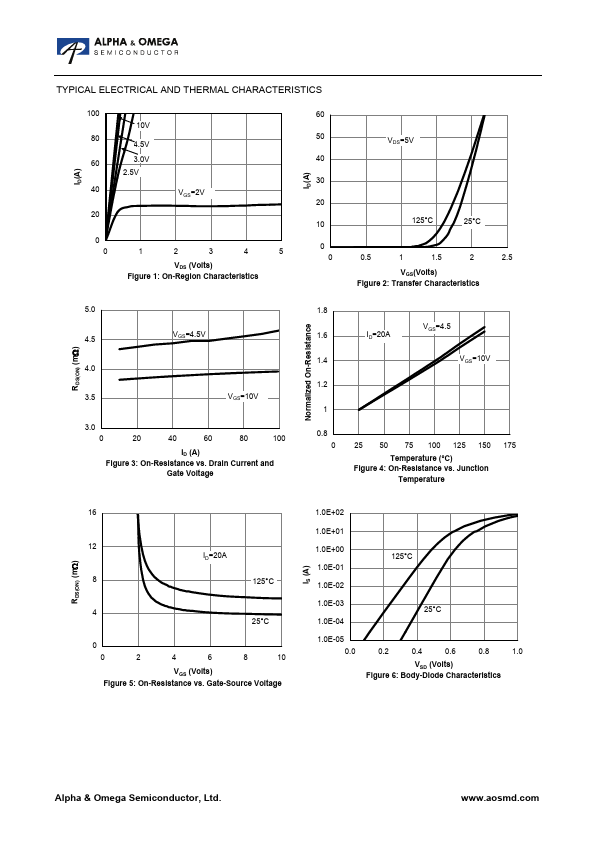
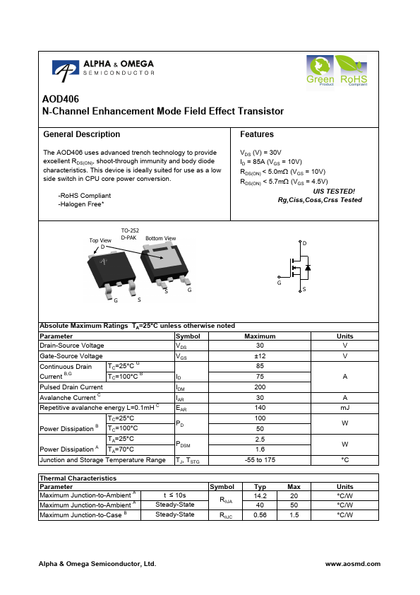
Datasheet4U Logo Datasheet4U.com

AOD406 - N-Channel Enhancement Mode Field Effect Transistor

Description

The AOD406 uses advanced trench technology to provide excellent RDS(ON), shoot-through immunity and body diode characteristics.

This device is ideally suited for use as a low side switch in CPU core power conversion.

Features

  • es VDS (V) = 30V ID = 85A (VGS = 10V) RDS(ON) < 5.0mΩ (VGS = 10V) RDS(ON) < 5.7mΩ (VGS = 4.5V) UIS TESTED! Rg,Ciss,Coss,Crss Tested TO-252 Top View D D-PAK Bottom View D G S S G G S Absolute Maximum Ratings TA=25°C unless otherwise noted Parameter Symbol Drain-Source Voltage VDS Gate-Source Voltage VGS Continuous Drain TC=25°C G Current B,G TC=100°C B ID Pulsed Drain Current IDM Avalanche Current C IAR Repetitive avalanche energy L=0.1mH C EAR TC=25°C Power Dissipati.

📥 Download Datasheet

Datasheet preview – AOD406

Datasheet Details

Part number AOD406
Manufacturer Alpha & Omega Semiconductors
File Size 304.88 KB
Description N-Channel Enhancement Mode Field Effect Transistor
Datasheet download datasheet AOD406 Datasheet
Additional preview pages of the AOD406 datasheet.
Other Datasheets by Alpha & Omega Semiconductors

Full PDF Text Transcription

Click to expand full text
AOD406 N-Channel Enhancement Mode Field Effect Transistor General Description The AOD406 uses advanced trench technology to provide excellent RDS(ON), shoot-through immunity and body diode characteristics. This device is ideally suited for use as a low side switch in CPU core power conversion. -RoHS Compliant -Halogen Free* Features VDS (V) = 30V ID = 85A (VGS = 10V) RDS(ON) < 5.0mΩ (VGS = 10V) RDS(ON) < 5.7mΩ (VGS = 4.5V) UIS TESTED! Rg,Ciss,Coss,Crss Tested TO-252 Top View D D-PAK Bottom View D G S S G G S Absolute Maximum Ratings TA=25°C unless otherwise noted Parameter Symbol Drain-Source Voltage VDS Gate-Source Voltage VGS Continuous Drain TC=25°C G Current B,G TC=100°C B ID Pulsed Drain Current IDM Avalanche Current C IAR Repetitive avalanche energy L=0.
Published: |