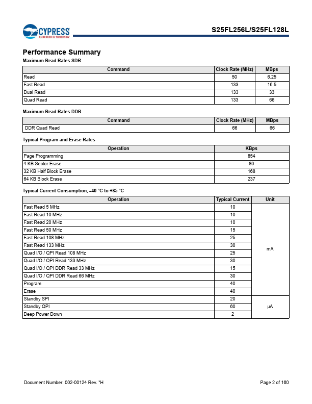
Datasheet4U Logo Datasheet4U.com

S25FL128L - 3.0V FL-L Flash Memory

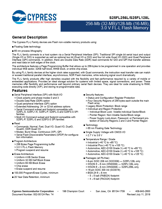
This page provides the datasheet information for the S25FL128L, a member of the S25FL256L 3.0V FL-L Flash Memory family.

Datasheet Summary

Description

The Cypress FL-L Family devices are Flash non-volatile memory products using: Floating Gate technology

The FL-L family connects to a host system via a Serial Peripheral Interface (SPI).

Features

  • a Page Programming Buffer that allows up to 256-bytes to be programmed in one operation and provides individual 4KB sector, 32KB half block, 64KB block, or entire chip erase. By using FL-L family devices at the higher clock rates supported, with Quad commands, the instruction read transfer rate can ma.

📥 Download Datasheet

Datasheet preview – S25FL128L

Datasheet Details

Part number S25FL128L
Manufacturer Cypress
File Size 1.36 MB
Description 3.0V FL-L Flash Memory
Datasheet download datasheet S25FL128L Datasheet
Additional preview pages of the S25FL128L datasheet.
Other Datasheets by Cypress

Full PDF Text Transcription

Click to expand full text
S25FL256L/S25FL128L 256Mbit (32Mbyte)/128Mbit (16Mbyte), 3.0 V FL-L Flash Memory General Description The Cypress FL-L Family devices are Flash non-volatile memory products using: – Floating Gate technology – 65 nm process lithography The FL-L family connects to a host system via a Serial Peripheral Interface (SPI). Traditional SPI single bit serial input and output (Single I/O or SIO) is supported as well as optional two bit (Dual I/O or DIO) and four bit wide Quad I/O (QIO) and Quad Peripheral Interface (QPI) commands. In addition, there are Double Data Rate (DDR) read commands for QIO and QPI that transfer address and read data on both edges of the clock.
Published: |