Datasheet Details
| Part number | M14D1G1664A |
|---|---|
| Manufacturer | ESMT |
| File Size | 1.98 MB |
| Description | DDR-II SDRAM |
| Datasheet |
 M14D1G1664A-ESMT.pdf M14D1G1664A-ESMT.pdf
|
| Part number | M14D1G1664A |
|---|---|
| Manufacturer | ESMT |
| File Size | 1.98 MB |
| Description | DDR-II SDRAM |
| Datasheet |
M14D1G1664A-ESMT.pdf
|
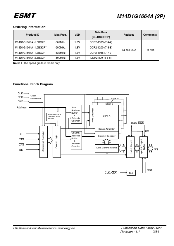
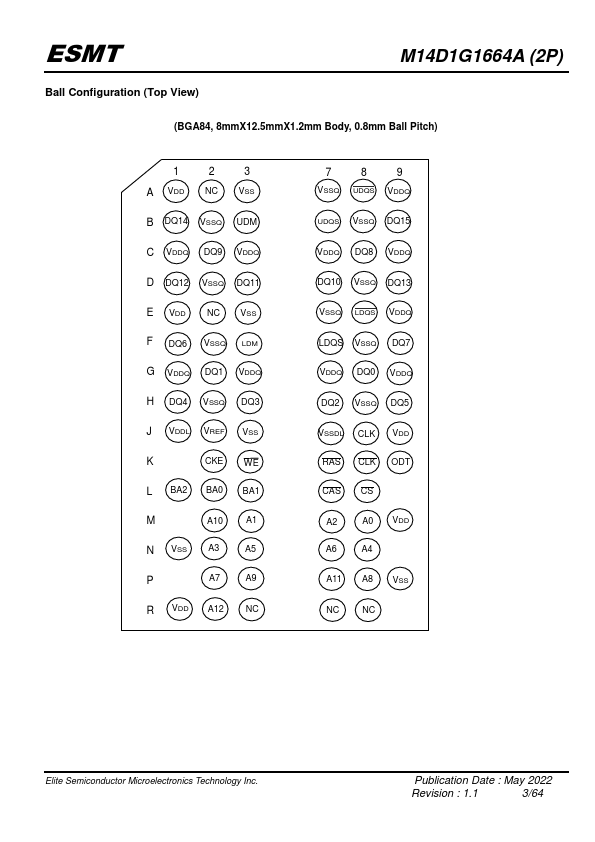
Pin Name A0~A12, BA0~BA2 DQ0~DQ15 RAS CAS WE VSS VDD DQS, DQS (LDQS, LDQS UDQS, UDQS) ODT NC Function Address inputs - Row address A0~A12 - Column address A0~A9 A10/AP : Auto Precharge BA0~BA2 : Bank selects (8 Banks) Data-in/Data-out Command input Command input Command input Ground Power Bi-directional differential Data Strobe.LDQS and LDQS are DQS for DQ0~DQ7; UDQS and UDQSare DQS for DQ8~DQ15. On-Die-Termination.ODT is only applied to DQ0~DQ15, DM, DQS and DQS .No connection Pin Name F
📁 M14D1G1664A Similar Datasheet