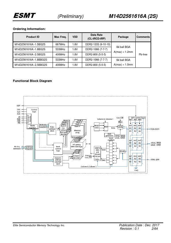
Description
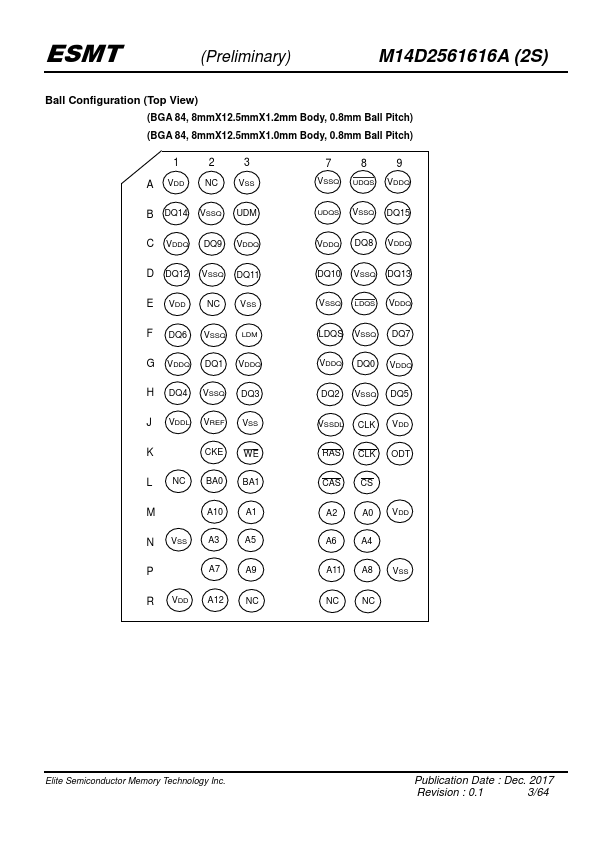
Ball Name
A0~A12, BA0,BA1
DQ0~DQ15 RAS CAS WE VSS VDD
DQS, DQS (LDQS, LDQS UDQS, UDQS )
ODT
NC
Function
Address inputs - Row address A0~A12 - Column address A0~A8 A10/AP : Auto Precharge BA0, BA1 : Bank selects (4 Banks)
Data-in/Data-out
Command input Command input Command input Ground Power
Bi-directional differential Data Strobe.LDQS and LDQS are DQS for DQ0~DQ7; UDQS and UDQS are DQS for DQ8~DQ15.
On-Die-Termination.ODT is only applied to DQ0~DQ15, DM, DQS and DQS .No connection
Ball Na
Features
- JEDEC Standard VDD = 1.8V ± 0.1V, VDDQ = 1.8V ± 0.1V Internal pipelined double-data-rate architecture; two data access per clock cycle Bi-directional differential data strobe (DQS, DQS ); DQS can be disabled for single-ended data strobe operation. On-chip DLL Differential clock inputs (CLK and CLK ) DLL aligns DQ and DQS transition with CLK transition 1KB page size - Row address: A0 to A12 - Column address: A0 to A8 Quad bank operation CAS Latency : 3, 4, 5, 6, 7, 8, 9 Additive Latency: 0, 1, 2,.
 M14D2561616A-ESMT.pdf