Datasheet Details
| Part number | M14F5121632A |
|---|---|
| Manufacturer | ESMT |
| File Size | 1.95 MB |
| Description | DDR II SDRAM |
| Datasheet |
 M14F5121632A-ESMT.pdf M14F5121632A-ESMT.pdf
|
|
|
The M14F5121632A by ESMT is a DDR II SDRAM. Below is the official datasheet preview.
| Part number | M14F5121632A |
|---|---|
| Manufacturer | ESMT |
| File Size | 1.95 MB |
| Description | DDR II SDRAM |
| Datasheet |
M14F5121632A-ESMT.pdf
|
|
|
|
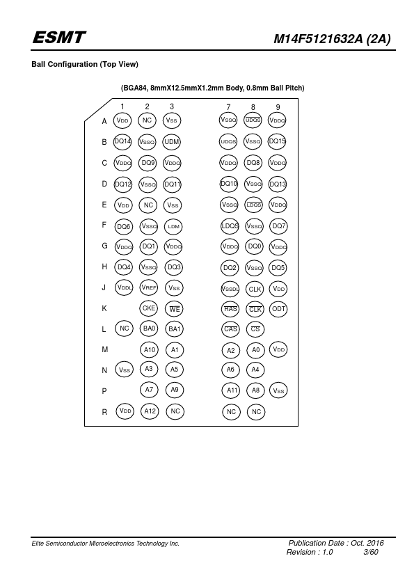
Pin Name A0~A12, BA0,BA1 DQ0~DQ15 RAS CAS WE VSS VDD DQS, DQS (LDQS, LDQS UDQS, UDQS) ODT NC Function Address inputs - Row address A0~A12 - Column address A0~A9 A10/AP : Auto Precharge BA0, BA1 : Bank selects (4 Banks) Data-in/Data-out Command input Command input Command input Ground Power Pin Name Function DM (LDM, UDM) DM is an input mask signal for write data.LDM is DM for DQ0~DQ7 and UDM is DM for DQ8~DQ15. CLK, CLK CKE CS VDDQ VSSQ VREF Differential clock input Clock enable Chip se
📁 M14F5121632A Similar Datasheet