Description
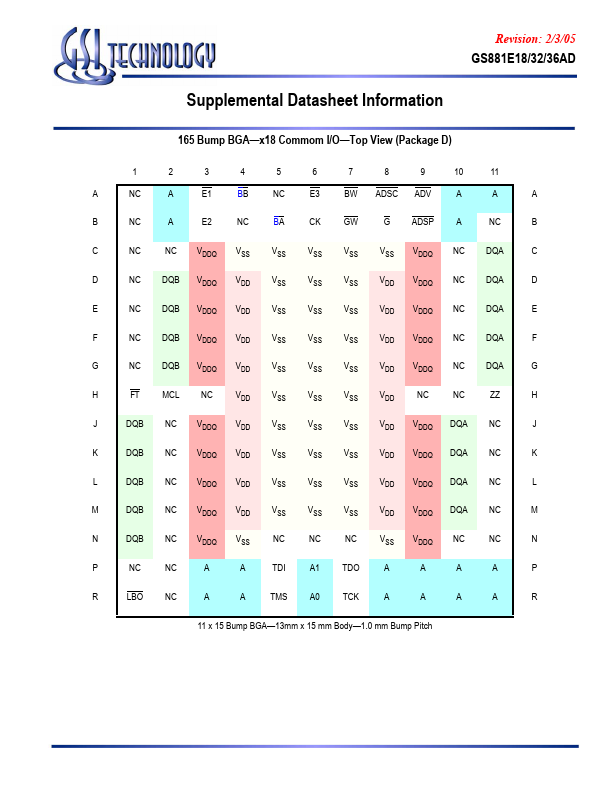
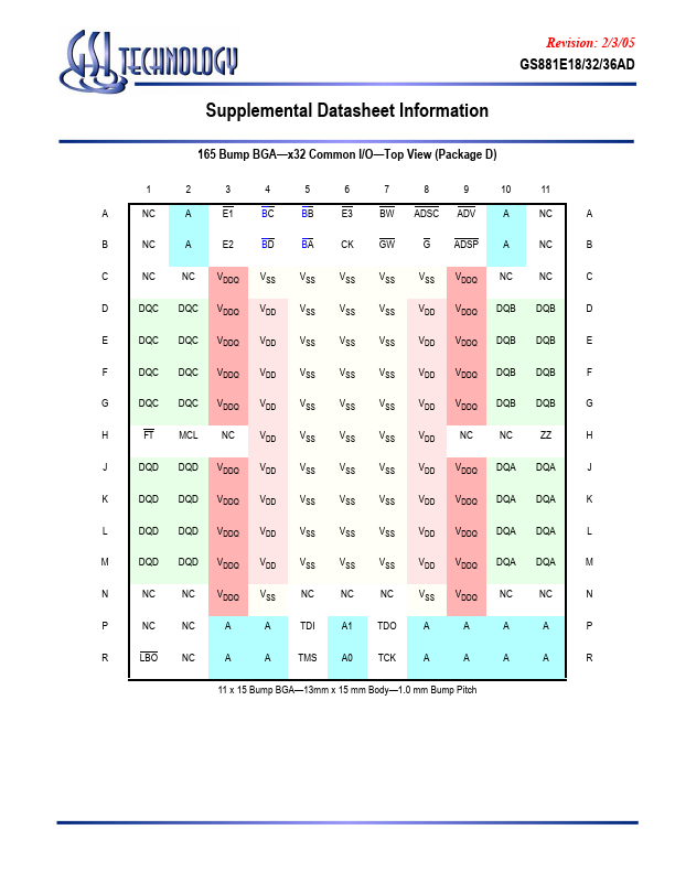
www.DataSheet4U.com Revision: 2/3/05 GS881E18/32/36AD Supplemental Datasheet Information This supplemental information applies to the GS881E18/36AT.
Symbol
A 0, A 1 An A17, A18 DQA1.
DQA9 DQB1.
DQB9 DQC1.
DQC9 DQD1.
DQD9 BA , BB , BC , BD NC CK BW GW E1 E3 E2 G ADV ADSC,.
Features
* only some of which are covered in this data sheet. See the GSI Technology web site (www. gsitechnology. com) for a complete listing of current offerings
Revision: 2/3/05
GS881E18/32/36AD
Supplemental Datasheet Information
Ordering Information Org
256K x 32 256K x 32 256K x 32 256K x 32 256K x 36 2
Applications
* JEDEC-standard package
512K x 18, 256K x 36 9Mb Synchronous Burst SRAMs
250 MHz
* 133 MHz 2.5 V or 3.3 V VDD 2.5 V or 3.3 V I/O
Flow Through/Pipeline Reads The function of the Data Output register can be controlled by the user via the FT mode pin (Pin 14). Holding the FT mode pin