Description
Symbol
Description
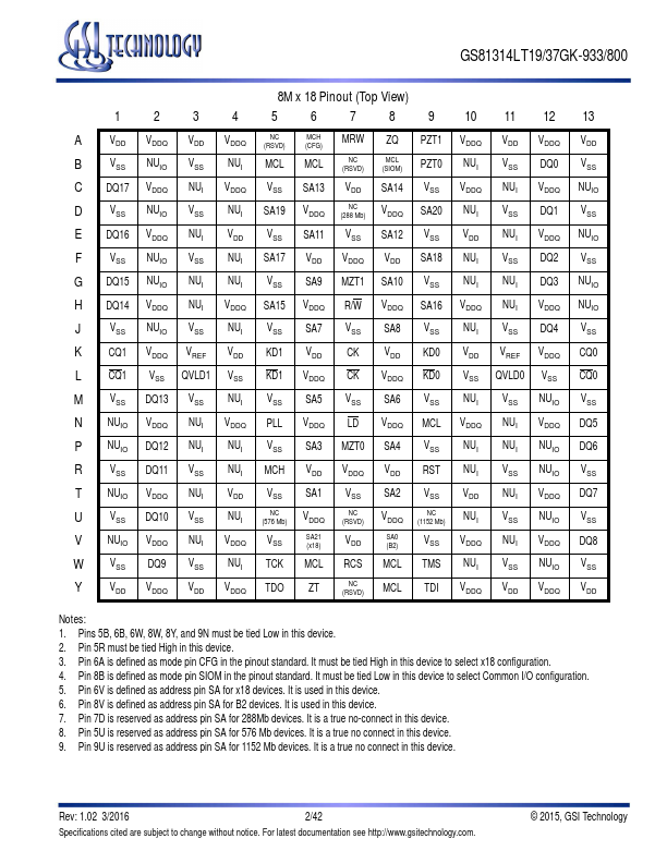
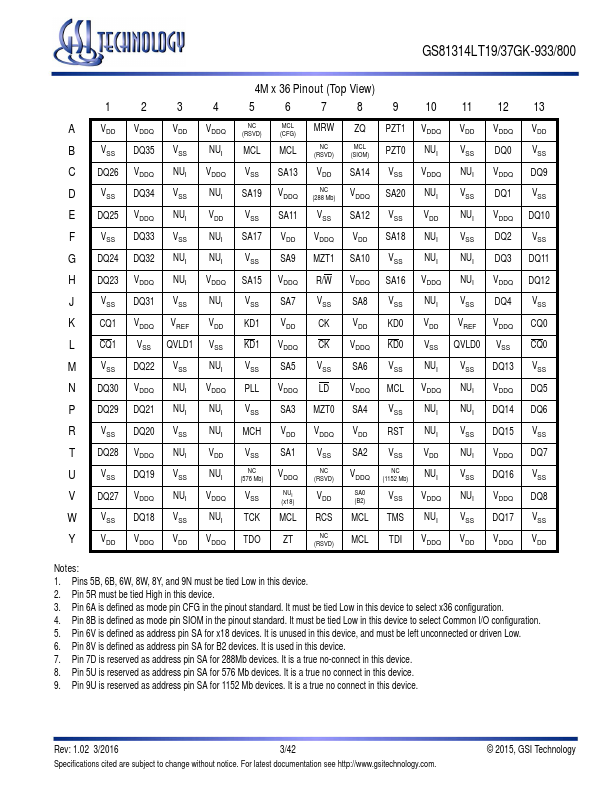
SA[21:0]
DQ[35:0]
QVLD[1:0] CK, CK KD[1:0], KD[1:0]
CQ[1:0], CQ[1:0]
LD R/W MRW
PLL
RST ZQ ZT RCS
MZT[1:0]
Address
Read or write address is registered on CK.
Registered on KD and KD during Write operations; aligned with CQ and CQ during Read operations.
Driven high one half cycle before valid read data.
Dual single-ended.
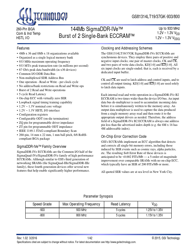
Features
- 4Mb x 36 and 8Mb x 18 organizations available.
- Organized as a single logical memory bank.
- 933 MHz maximum operating frequency.
- 933 MT/s peak transaction rate (in millions per second).
- 67 Gb/s peak data bandwidth (in x36 devices).
- Common I/O DDR Data Bus.
- Non-multiplexed SDR Address Bus.
- One operation - Read or Write - per clock cycle.
- No address/bank restrictions on Read and Write ops.
- Burst of 2 Read and.


