2SK291
Silicon N-Channel Junction FET
Application
Low frequency low noise amplifier
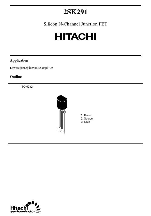
Outline
TO-92 (2)
1. Drain 2. Source 3. Gate 3 2 1
Absolute Maximum Ratings (Ta = 25°C)
Item Gate to drain voltage Gate to source voltage Drain current Gate current Channel power dissipation Channel temperature Storage temperature Symbol VGDO VGSO ID IG Pch Tch Tstg Ratings
- 15
- 15 50 5 300 150
- 55 to +150 Unit V V m A m A m W °C °C
Electrical Characteristics (Ta = 25°C)
Item Gate to drain breakdown voltage Gate to source breakdown voltage Gate cutoff current Drain current Gate to source cutoff voltage Forward transfer admittance Input capacitance Symbol V(BR)GDO V(BR)GSO I GSS I DSS-
Min
- 15
- 15
- 5
- 25
- -
Typ
- -
- -
- 45 8.5 1.2
Max
- - 10 50
- 3.0
- -
- Unit V V n A m A V m S p F
Test conditions I G =
- 100 µA I G =
- 100 µA VGS =
- 7 V, VDS = 0 VDS = 5 V, VGS = 0 VDS = 5 V, ID = 100 µA VDS = 5 V, VGS = 0, f = 1 k Hz VDS = 5 V, VGS = 0, f = 1 MHz
VGS(off) |yfs| Ciss
Noise voltage...