Datasheet Details
| Part number | HD74ACT107 |
|---|---|
| Manufacturer | Hitachi Semiconductor |
| File Size | 57.91 KB |
| Description | Dual JK Flip-Flop (with Separate Clear and Clock) |
| Datasheet |
 HD74ACT107 Datasheet HD74ACT107 Datasheet
|

|
|
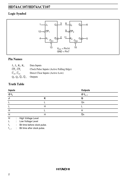
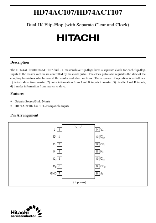
The HD74AC107/HD74ACT107 dual JK master/slave flip-flops have a separate clock for each flip-flop.
Inputs to the master section are controlled by the clock pulse.
The clock pulse also regulates the state of the coupling transistors which connect the master and slave sections.
| Part number | HD74ACT107 |
|---|---|
| Manufacturer | Hitachi Semiconductor |
| File Size | 57.91 KB |
| Description | Dual JK Flip-Flop (with Separate Clear and Clock) |
| Datasheet |
HD74ACT107 Datasheet
|
|
|
|