High Speed Operation: tpd = 11 ns typ (CL = 50 pF) High Output Current: Fanout of 10 LSTTL Loads Wide Operating Voltage: VCC = 2 to 6 V Low Input Current: 1 µA max Low Quiescent Supply Current: ICC (static) = 1 µA max (Ta = 25°C)
Pin Arrangement
A B C D E F GND
1 2 3 4 5 6 7 (Top view)
14 VCC 13 NC 12 H 11 G 10 NC 9 8 NC Y
HD74HC30
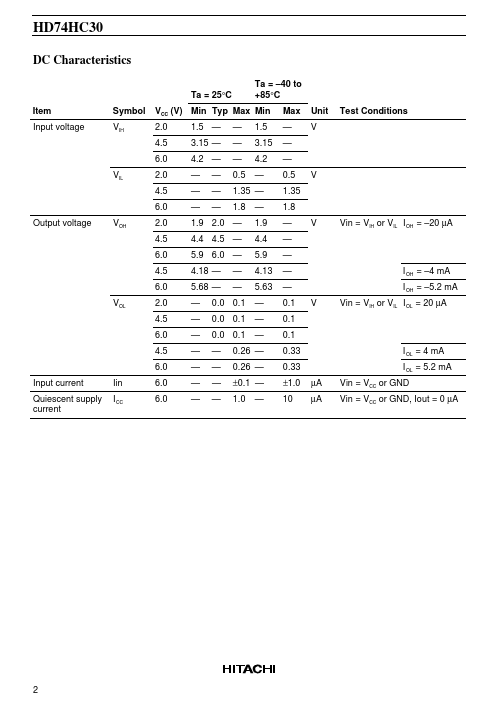
DC Characteristics
Ta = 25°C Item Input voltage Symbol VIH Ta =.
HD74HC30
8-input NAND Gate
Features
• • • • • High Speed Operation: tpd = 11 ns typ (CL = 50 pF) High Output Current: Fanout of 10 LSTTL Loads Wide Operating Voltage: VCC = 2 to 6 V Low Input Current: 1 µA max Low Quiescent Supply Current: ICC (static) = 1 µA max (Ta = 25°C)
Pin Arrangement
A B C D E F GND
1 2 3 4 5 6 7 (Top view)
14 VCC 13 NC 12 H 11 G 10 NC 9 8 NC Y
HD74HC30
DC Characteristics
Ta = 25°C Item Input voltage Symbol VIH Ta = –40 to +85°C Max — — — 0.5 1.35 1.8 — — — — — 0.1 0.1 0.1 0.33 0.33 ±1.0 10 µA µA I OL = 4 mA I OL = 5.2 mA Vin = VCC or GND Vin = VCC or GND, Iout = 0 µA V I OH = –4 mA I OH = –5.2 mA Vin = VIH or VIL I OL = 20 µA V Vin = VIH or VIL I OH = –20 µA V Unit V Test Conditions
VCC (V) Min Typ Max Min 2.0 4.5 6.0 1.5 — 3.15 — 4.2 — — — — — — — — — — 0.
 HD74HC30 Datasheet