Datasheet Details
| Part number | HD74LV574A |
|---|---|
| Manufacturer | Hitachi Semiconductor |
| File Size | 68.42 KB |
| Description | Octal Edge-Triggered D-type Flip-Flops with 3-state Outputs |
| Datasheet |
 HD74LV574A Datasheet HD74LV574A Datasheet
|
|
|
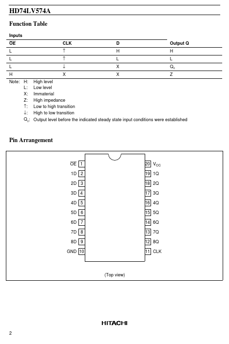
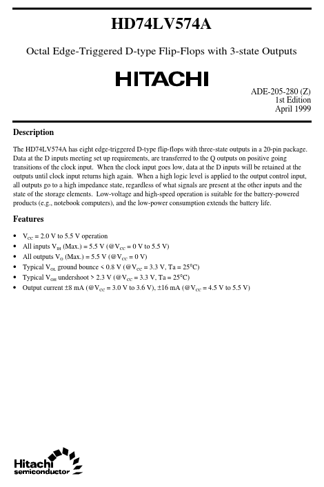
The HD74LV574A has eight edge-triggered D-type flip-flops with three-state outputs in a 20-pin package.
Data at the D inputs meeting set up requirements, are transferred to the Q outputs on positive going transitions of the clock input.
| Part number | HD74LV574A |
|---|---|
| Manufacturer | Hitachi Semiconductor |
| File Size | 68.42 KB |
| Description | Octal Edge-Triggered D-type Flip-Flops with 3-state Outputs |
| Datasheet |
HD74LV574A Datasheet
|
|
|
|