Datasheet Details
| Part number | HY5V66GF |
|---|---|
| Manufacturer | Hynix Semiconductor |
| File Size | 235.30 KB |
| Description | 4 Banks X 1M X 16Bit Synchronous DRAM |
| Datasheet |
 HY5V66GF_HynixSemiconductor.pdf HY5V66GF_HynixSemiconductor.pdf
|
|
|
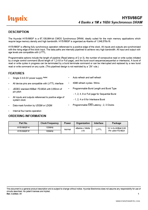
The HY5V66GF by Hynix Semiconductor is a 4 Banks X 1M X 16Bit Synchronous DRAM. Below is the official datasheet preview.
| Part number | HY5V66GF |
|---|---|
| Manufacturer | Hynix Semiconductor |
| File Size | 235.30 KB |
| Description | 4 Banks X 1M X 16Bit Synchronous DRAM |
| Datasheet |
HY5V66GF_HynixSemiconductor.pdf
|
|
|
|
The Hyundai HY5V66GF is a 67,108,864-bit CMOS Synchronous DRAM, ideally suited for the main memory applications which require large memory density and high bandwidth.
📁 HY5V66GF Similar Datasheet