Datasheet4U Logo Datasheet4U.com

CD4093BMS - CMOS Quad 2-Input NAND Schmitt Triggers

Datasheet Summary

Description

of ‘B’ Series CMOS Devices” A 1 B 2 J=A B 3 K=C D 4 C 5 D 6 VSS 7 14 VDD 13 H 12 G 11 M = G H 10 L = E F 9 F 8 E Functional Diagram Applications Wave and Pulse Shapers High Noise Environment Systems Monostable Multivibrators Astable Mul

Features

  • High Voltage Types (20V Rating).
  • Schmitt Trigger Action on Each Input With No External Components.
  • Hysteresis Voltage Typically 0.9V at VDD = 5V and 2.3V at VDD = 10V.
  • Noise Immunity Greater than 50%.
  • No Limit on Input Rise and Fall Times.
  • Standardized, Symmetrical Output Characteristics.
  • 100% Tested for Quiescent Current at 20V.
  • Maximum Input Current of 1µA at 18V Over Full Package Temperature Range, 100nA at 18V and +25oC.

📥 Download Datasheet

Datasheet preview – CD4093BMS

Datasheet Details

Part number CD4093BMS
Manufacturer Intersil Corporation
File Size 278.48 KB
Description CMOS Quad 2-Input NAND Schmitt Triggers
Datasheet download datasheet CD4093BMS Datasheet
Additional preview pages of the CD4093BMS datasheet.
Other Datasheets by Intersil Corporation

Full PDF Text Transcription

Click to expand full text
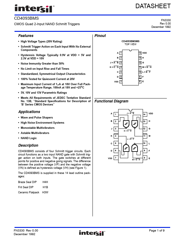
CD4093BMS December 1992 CMOS Quad 2-Input NAND Schmitt Triggers Pinout CD4093BMSMS TOP VIEW Features • High Voltage Types (20V Rating) • Schmitt Trigger Action on Each Input With No External Components • Hysteresis Voltage Typically 0.9V at VDD = 5V and 2.3V at VDD = 10V • Noise Immunity Greater than 50% • No Limit on Input Rise and Fall Times • Standardized, Symmetrical Output Characteristics • 100% Tested for Quiescent Current at 20V • Maximum Input Current of 1µA at 18V Over Full Package Temperature Range, 100nA at 18V and +25oC • 5V, 10V and 15V Parametric Ratings • Meets All Requirements of JEDEC Tentative Standard No.
Published: |