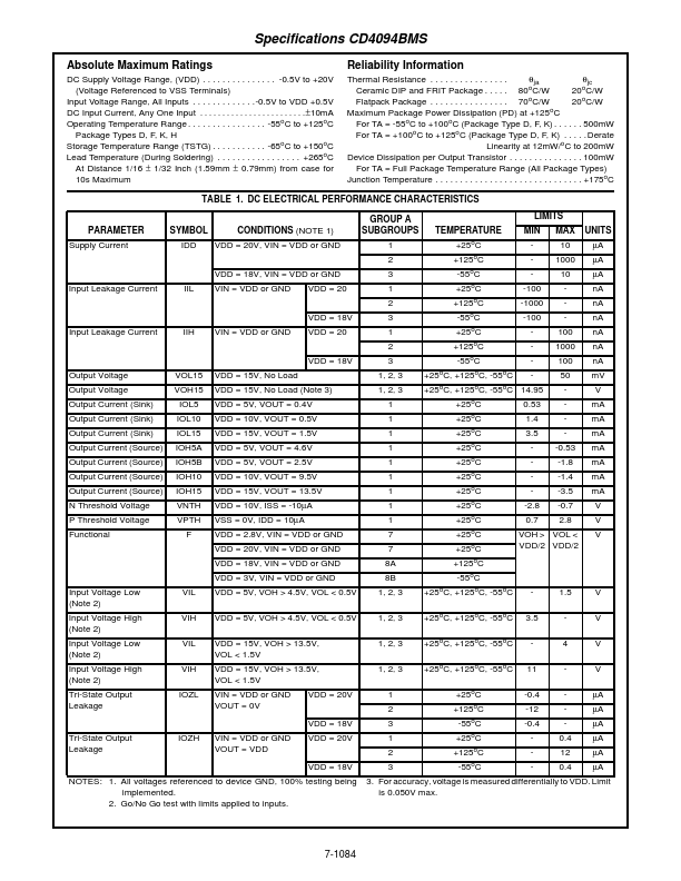
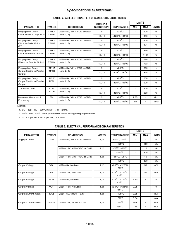
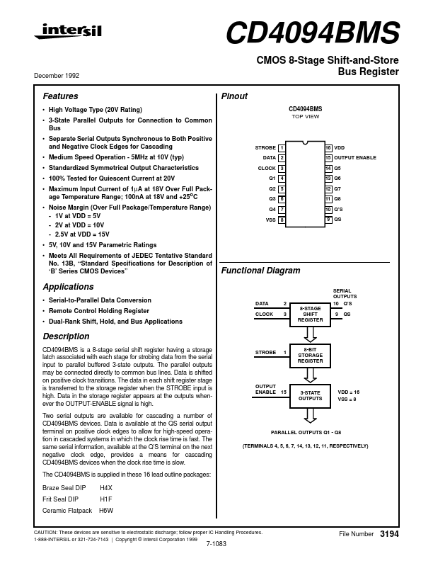
Datasheet4U Logo Datasheet4U.com

CD4094BMS - CMOS 8-Stage Shift-and-Store Bus Register

Datasheet Summary

Description

of ‘B’ Series CMOS Devices” STROBE 1 DATA 2 CLOCK Q1 Q2 Q3 Q4 VSS 3 4 5 6 7 8 16 VDD 15 OUTPUT ENABLE 14 Q5 13 Q6 12 Q7 11 Q8 10 Q’S 9 QS Functional Diagram SERIAL OUTPUTS 10 Q’S 8-STAGE SHIFT REGISTER 9 QS Applications Serial-to-Parallel Data Conversion Remote Control Holdin

Features

  • High Voltage Type (20V Rating).
  • 3-State Parallel Outputs for Connection to Common Bus.
  • Separate Serial Outputs Synchronous to Both Positive and Negative Clock Edges for Cascading.
  • Medium Speed Operation - 5MHz at 10V (typ).
  • Standardized Symmetrical Output Characteristics.
  • 100% Tested for Quiescent Current at 20V.
  • Maximum Input Current of 1µA at 18V Over Full Package Temperature Range; 100nA at 18V and +25oC.
  • Noise Margin (O.

📥 Download Datasheet

Datasheet preview – CD4094BMS

Datasheet Details

Part number CD4094BMS
Manufacturer Intersil Corporation
File Size 87.80 KB
Description CMOS 8-Stage Shift-and-Store Bus Register
Datasheet download datasheet CD4094BMS Datasheet
Additional preview pages of the CD4094BMS datasheet.
Other Datasheets by Intersil Corporation

Full PDF Text Transcription

Click to expand full text
CD4094BMS December 1992 CMOS 8-Stage Shift-and-Store Bus Register Pinout CD4094BMS TOP VIEW Features • High Voltage Type (20V Rating) • 3-State Parallel Outputs for Connection to Common Bus • Separate Serial Outputs Synchronous to Both Positive and Negative Clock Edges for Cascading • Medium Speed Operation - 5MHz at 10V (typ) • Standardized Symmetrical Output Characteristics • 100% Tested for Quiescent Current at 20V • Maximum Input Current of 1µA at 18V Over Full Package Temperature Range; 100nA at 18V and +25oC • Noise Margin (Over Full Package/Temperature Range) - 1V at VDD = 5V - 2V at VDD = 10V - 2.5V at VDD = 15V • 5V, 10V and 15V Parametric Ratings • Meets All Requirements of JEDEC Tentative Standard No.
Published: |