Datasheet Details
| Part number | CD4504BMS |
|---|---|
| Manufacturer | Intersil Corporation |
| File Size | 60.51 KB |
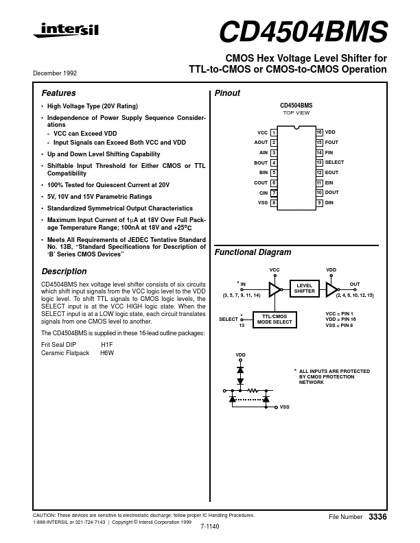
| Description | CMOS Hex Voltage Level Shifter for TTL-to-CMOS or CMOS-to-CMOS Operation |
| Datasheet |
 CD4504BMS Datasheet CD4504BMS Datasheet
|
|
|
| Part number | CD4504BMS |
|---|---|
| Manufacturer | Intersil Corporation |
| File Size | 60.51 KB |
| Description | CMOS Hex Voltage Level Shifter for TTL-to-CMOS or CMOS-to-CMOS Operation |
| Datasheet |
CD4504BMS Datasheet
|
|
|
|