Click to expand full text
N-Channel 20V MOSFET
LTC2312
Features: Surface-mounted package High Density Cell Design Halogen free
Application Ultra Low On-Resistance
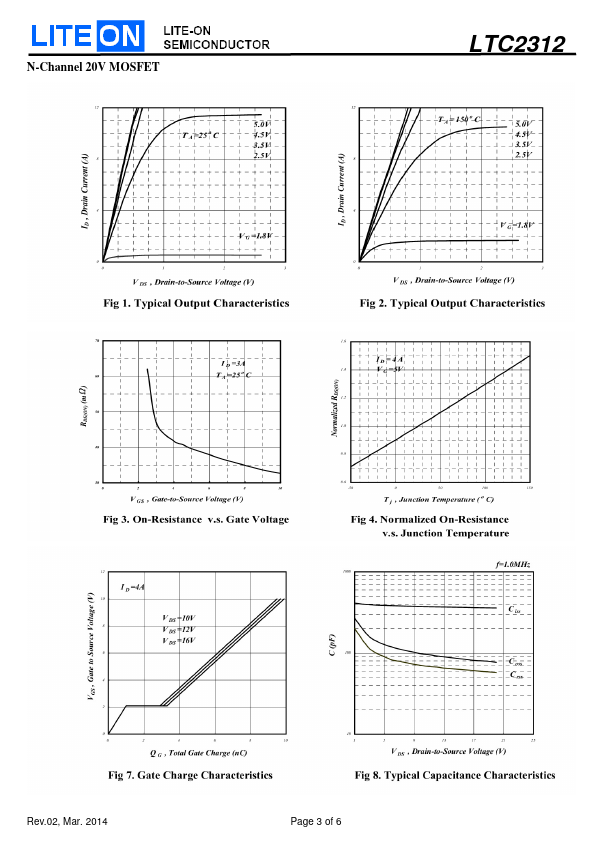
BVDSS= 20V , RDS(ON)< 41mΩ@VGS= 4.5V RDS(ON)< 47mΩ@VGS= 2.5V RDS(ON)< 57mΩ@VGS= 1.8V ID= 4.9A
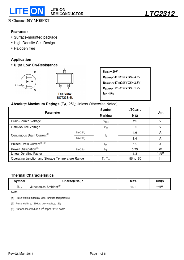
Absolute Maximum Ratings (TA=25℃Unless Otherwise Noted)
Parameter
Symbol Marking
Drain-Source Voltage
VDSS
Gate-Source Voltage Continuous Drain Current(3)
℃Ta=25 ℃Ta=70
Pulsed Drain Current(1、2) Power Dissipation(1) Linear Derating Factor
℃Ta=25
Operating Junction and Storage Temperature Range
VGS ID IDM PD
TJ, Tstg
LTC2312 N12 20 ±8 4.9 3.4 15 0.75 1.3
-55 to150
Unit
V V A A A
℃W /W ℃
Thermal Characteristics
Symbol
RθJA
:Note
Characteristic Junction-to-Ambient(3)
(1) Pulse width limited by Max.
 LTC2312 Datasheet