Datasheet Details
| Part number | SN74LS109A |
|---|---|
| Manufacturer | Motorola |
| File Size | 147.54 KB |
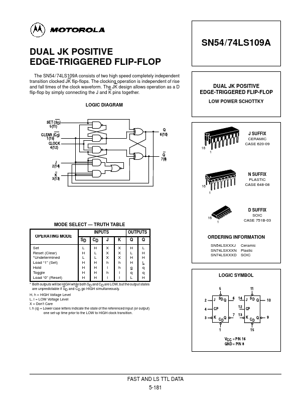
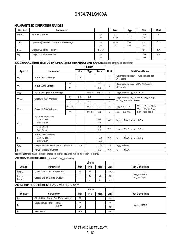
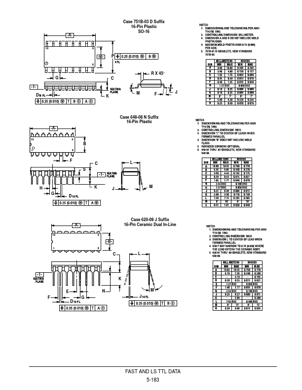
| Description | DUAL JK POSITIVE EDGE-TRIGGERED FLIP-FLOP |
| Datasheet |
 SN74LS109A Datasheet SN74LS109A Datasheet
|
| Note |
This datasheet PDF includes multiple part numbers: SN74LS109A, SN74LS109. Please refer to the document for exact specifications by model. |
|
|