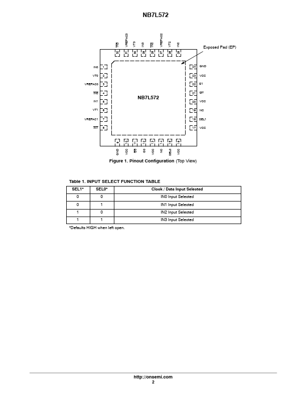
Description
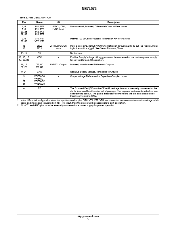
Pin
Name
I/O
Description
1, 4 5, 8 25, 28 29, 32
IN0, IN0 IN1, IN1 IN2, IN2 IN3, IN3
LVPECL, CML, Non
inverted, Inverted, Differential Clock or Data Inputs.
tapped Termination Pin for INx / INx
15 18
14, 19
SEL0 SEL1
NC
LVTTL/LVCMOS Input
Input Select pins, default HIGH when left open through a 28k
W pull
up resistor.
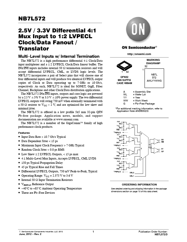
Features
- Input Data Rate > 10.7 Gb/s Typical.
- Data Dependent Jitter < 15 ps.
- Maximum Input Clock Frequency > 7 GHz Typical.
- Random Clock Jitter < 0.8 ps RMS.
- Low Skew 1:2 LVPECL Outputs, < 15 ps max.
- 4:1 Multi.
- Level Mux Inputs, Accepts LVPECL, CML LVDS.
- 150 ps Typical Propagation Delay.
- 45 ps Typical Rise and Fall Times.
- Differential LVPECL Outputs, 750 mV Peak-to-Peak, Typical.
- Operating Range: VCC = 2.375.
 NB7L572 Datasheet