Datasheet Details
| Part number | NB7L585 |
|---|---|
| Manufacturer | ON Semiconductor |
| File Size | 88.05 KB |
| Description | Differential 1:6 LVPECL Clock/Data distribution |
| Datasheet |
 NB7L585 Datasheet NB7L585 Datasheet
|
|
|
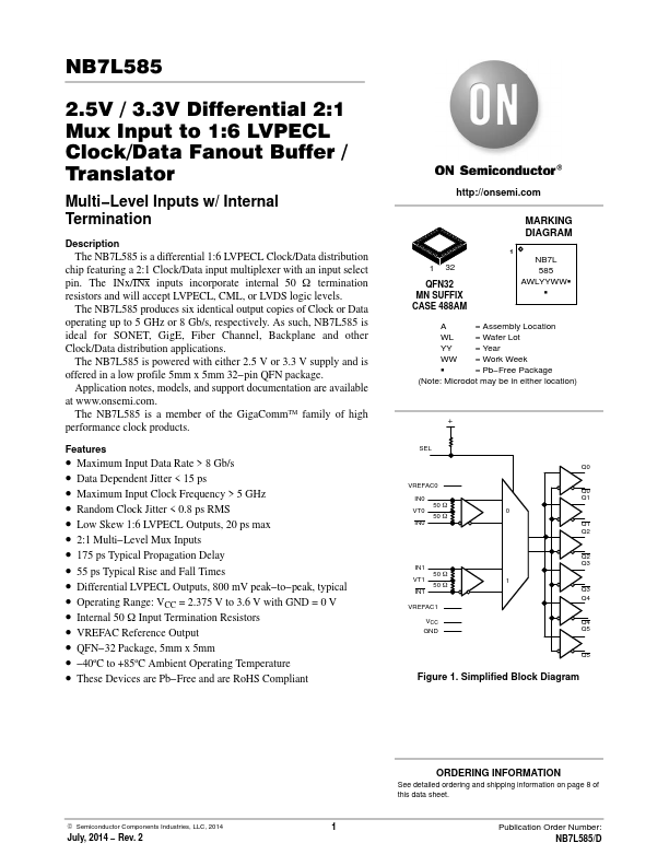
chip featuring a 2:1 Clock/Data input multiplexer with an input select pin.
The INx/INx inputs incorporate internal 50 W termination resistors and will accept LVPECL, CML, or LVDS logic levels.
| Part number | NB7L585 |
|---|---|
| Manufacturer | ON Semiconductor |
| File Size | 88.05 KB |
| Description | Differential 1:6 LVPECL Clock/Data distribution |
| Datasheet |
NB7L585 Datasheet
|
|
|
|