Datasheet Details
| Part number | NCP1593A |
|---|---|
| Manufacturer | ON Semiconductor ↗ |
| File Size | 479.46 KB |
| Description | Synchronous Buck Regulator |
| Datasheet |
 NCP1593A_ONSemiconductor.pdf NCP1593A_ONSemiconductor.pdf
|
| Part number | NCP1593A |
|---|---|
| Manufacturer | ON Semiconductor ↗ |
| File Size | 479.46 KB |
| Description | Synchronous Buck Regulator |
| Datasheet |
NCP1593A_ONSemiconductor.pdf
|
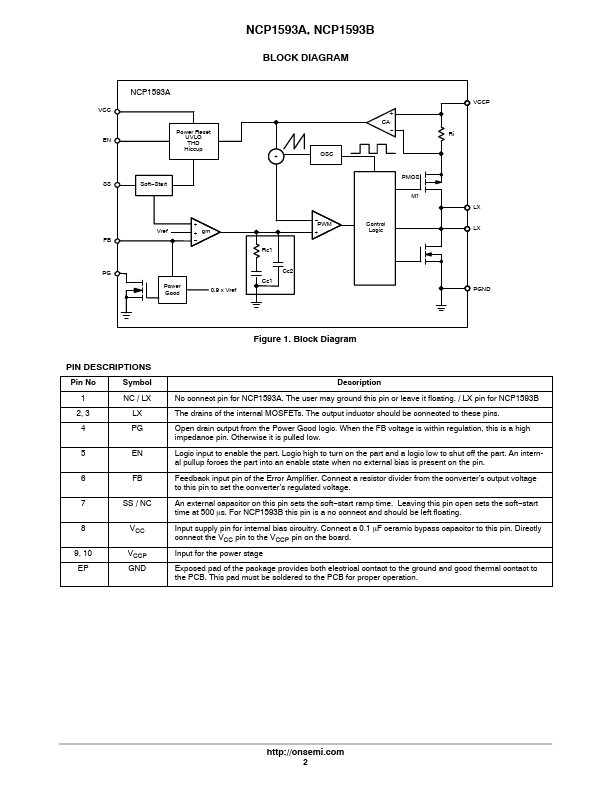
Pin No Symbol 1 NC / LX 2, 3 LX 4 PG 5 EN 6 FB 7 SS / NC 8 9, 10 EP VCC VCCP GND Figure 1. Block Diagram Description No connect pin for NCP1593A.The user may ground this pin or leave it floating./ LX pin for NCP1593B The drains of the internal MOSFETs.The output inductor should be connected to these pins.Open drain output from the Power Good logic.When the FB voltage is within regulation, this is a high impedance pin.Otherwise it is pulled low.Logic input to enable the part.L
📁 NCP1593A Similar Datasheet