Description
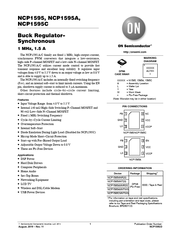
Pin No
Symbol
1 FB
2 GND 3 LX 4 VCCP 5 VCC
6 NC EN
EP PAD
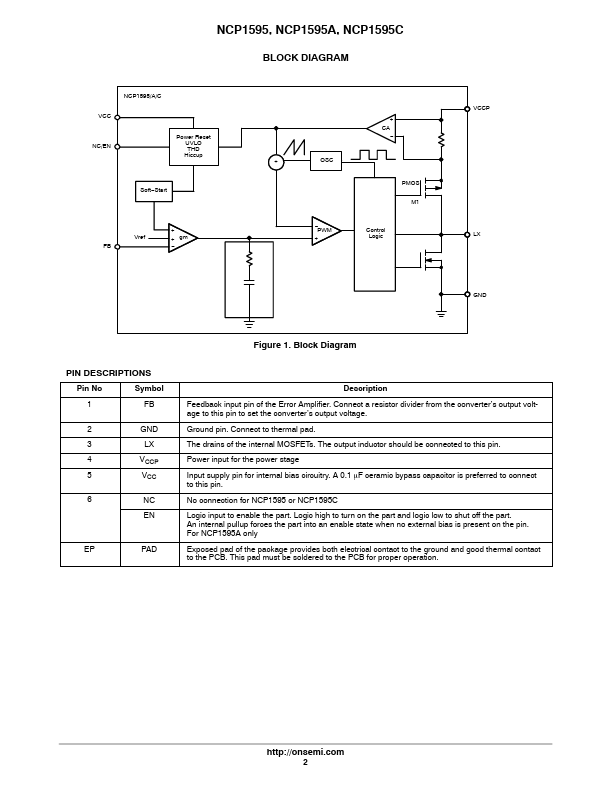
Figure 1. Block Diagram
Description Feedback input pin of the Error Amplifier.Connect a resistor divider from the converter’s output voltage to this pin to set the converter’s output voltage.Ground pin.Connect to thermal pad.The drains of the internal MOSFETs.The output inductor should be connected to this pin.Power input for the power stage Input supply pin for internal bias circuitry.A 0.1 mF ceramic bypass capacitor is pr
Features
- include cycle.
- by.
- cycle current limiting, short.
- circuit protection and thermal shutdown. Features.
- Input Voltage Range: from 4.0 V to 5.5 V.
- Internal 140 mW High.
- Side Switching P.
- Channel MOSFET and
90 mW Low.
- Side N.
- Channel MOSFET.
- Fixed 1 MHz Switching Frequency.
- Cycle.
- by.
- Cycle Current Limiting.
- Overtemperature Protection.
- Internal Soft.
- Start.
- Diode Emulat.
 NCP1595_ONSemiconductor.pdf