Description
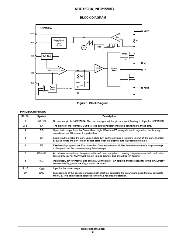
Pin No
Symbol
1 NC / LX
2, 3 LX
4 PG
5 EN
6 FB
7 SS / NC
8
9, 10 EP
VCC
VCCP GND
Figure 1. Block Diagram
Description No connect pin for NCP1593A.The user may ground this pin or leave it floating./ LX pin for NCP1593B The drains of the internal MOSFETs.The output inductor should be connected to these pins.Open drain output from the Power Good logic.When the FB voltage is within regulation, this is a high impedance pin.Otherwise it is pulled low.Logic input to enable the part.L
Features
- include cycle.
- by.
- cycle current limiting, 100% duty cycle operation, short.
- circuit protection, power saving mode and thermal shutdown. Features.
- Wide Input Voltage Range: from 4.0 V to 5.5 V.
- Internal 90 mW High.
- Side P.
- Channel MOSFET and 60 mW
Low.
- Side N.
- Channel MOSFET.
- Fixed 1 MHz Switching Frequency.
- Cycle.
- by.
- Cycle Current Limiting.
- Hiccup Mode Short.
- Circuit Protection.
 NCP1593A_ONSemiconductor.pdf