Datasheet Details
| Part number | NCP51530 |
|---|---|
| Manufacturer | ON Semiconductor ↗ |
| File Size | 1.22 MB |
| Description | High and Low Side Gate Driver |
| Datasheet |
 NCP51530-ONSemiconductor.pdf NCP51530-ONSemiconductor.pdf
|
| Part number | NCP51530 |
|---|---|
| Manufacturer | ON Semiconductor ↗ |
| File Size | 1.22 MB |
| Description | High and Low Side Gate Driver |
| Datasheet |
NCP51530-ONSemiconductor.pdf
|
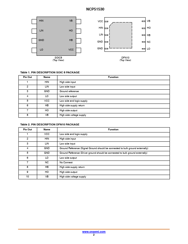
SOIC 8 PACKAGE Pin Out Name 1 HIN High side input 2 LIN Low side input 3 GND Ground reference 4 LO Low side output 5 VCC Low side and logic supply 6 HB High side supply return 7 HO High side output 8 VB High side voltage supply Function Table 2. PIN DESCRIPTION DFN10 PACKAGE Pin Out Name Function 1 VCC Low side and logic supply 2 HIN High side input 3 LIN Low side input 4 GND Ground Reference (Signal Ground should be connected to bulk ground externally)
📁 NCP51530 Similar Datasheet