Datasheet4U Logo Datasheet4U.com

NCP51510 Datasheet - ON Semiconductor

NCP51510 Termination Source / Sink Regulator

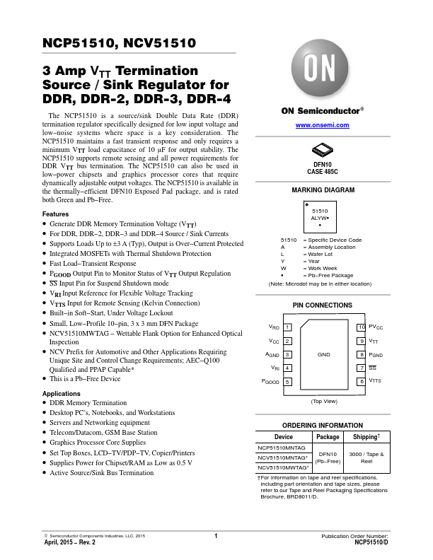
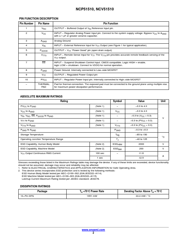
Pin Number Pin Name Pin Function 1 VRO OUTPUT * Buffered Output of VRI Reference Input pin. 2 VCC INPUT * Regulator Analog Power Input pin. Connect to the system supply voltage. Bypass VCC to AGND with a 1 mF or greater ceramic capacitor. 3 AGND Analog Ground 4 VRI INPUT <.
NCP51510, NCV51510 3 Amp VTT Termination Source / Sink Regulator for DDR, DDR-2, DDR-3, DDR-4 The NCP51510 is a source/sink Double Data Rate (DDR) termination regulator specifically designed for low input voltage and low noise systems where space is a key consideration. The NCP51510 maintains a fast transient response and only requires a minimum VTT load capacitance of 10 mF for output stability. The NCP51510 supports remote sensing and all power requirements for DDR VTT bus termination.

NCP51510 Features

* Generate DDR Memory Termination Voltage (VTT)

* For DDR, DDR

* 2, DDR

* 3 and DDR

* 4 Source / Sink Currents

* Supports Loads Up to ±3 A (Typ), Output is Over

* Current Protected

* Integrated MOSFETs with Thermal Shutdown Protection

NCP51510 Datasheet (141.75 KB)

Preview of NCP51510 PDF
NCP51510 Datasheet Preview Page 2 NCP51510 Datasheet Preview Page 3

Datasheet Details

Part number:

NCP51510

Manufacturer:

ON Semiconductor ↗

File Size:

141.75 KB

Description:

Termination source / sink regulator.

📁 Related Datasheet

NCP51530 High and Low Side Gate Driver (ON Semiconductor)

NCP51560 Dual Channel Gate Driver (ON Semiconductor)

NCP51561 Dual Channel Gate Driver (ON Semiconductor)

NCP51563 Dual Channel Gate Driver (ON Semiconductor)

NCP5104 Half Bridge Driver (ON Semiconductor)

NCP5106A High and Low Side Driver (ON Semiconductor)

NCP5106B High and Low Side Driver (ON Semiconductor)

NCP5109A High and Low Side Driver (ON Semiconductor)

TAGS

NCP51510 Termination Source Sink Regulator ON Semiconductor

NCP51510 Distributor