Click to expand full text
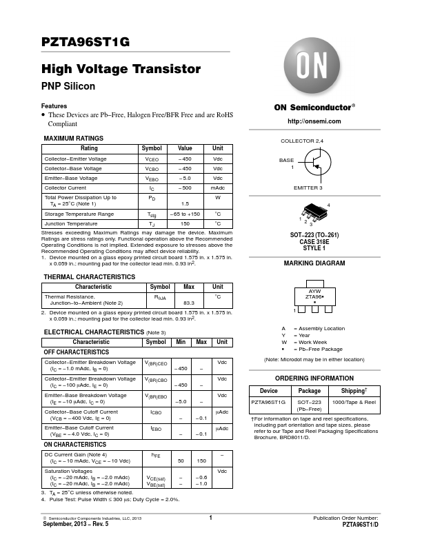
PZTA96ST1G
High Voltage Transistor
PNP Silicon
Features
• These Devices are Pb−Free, Halogen Free/BFR Free and are RoHS
Compliant
MAXIMUM RATINGS
Rating
Symbol
Value
Unit
Collector−Emitter Voltage
VCEO
− 450
Vdc
Collector−Base Voltage
VCBO
− 450
Vdc
Emitter−Base Voltage
VEBO
− 5.0
Vdc
Collector Current
IC
− 500
mAdc
Total Power Dissipation Up to TA = 25°C (Note 1)
PD W 1.5
Storage Temperature Range
Tstg − 65 to +150 °C
Junction Temperature
TJ 150 °C
Stresses exceeding Maximum Ratings may damage the device. Maximum
Ratings are stress ratings only. Functional operation above the Recommended
Operating Conditions is not implied. Extended exposure to stresses above the
Recommended Operating Conditions may affect device reliability.
1.
 PZTA96ST1G Datasheet