Datasheet4U Logo Datasheet4U.com

MN3814 Datasheet - Panasonic Semiconductor

MN3814_PanasonicSemiconductor.pdf
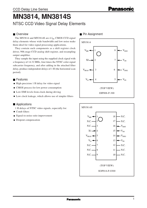
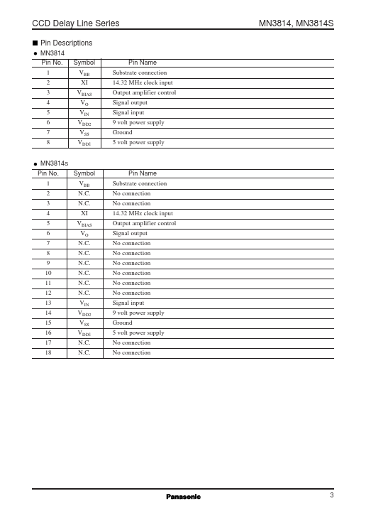
Preview of MN3814 PDF
MN3814 Datasheet Preview Page 2 MN3814 Datasheet Preview Page 3

Datasheet Details

Part number:

MN3814

Manufacturer:

Panasonic Semiconductor

File Size:

44.23 KB

Description:

Ntsc ccd video signal delay elements.

MN3814, NTSC CCD Video Signal Delay Elements

MN3814 Pin No.

1 2 3 4 5 6 7 8 MN3814S Pin No.

1 2 3 4 5 6 7 8 9 10 11 12 13 14 15 16 17 18 Symbol VBB N.C.

N.C.

XI VBIAS VO N.C.

N.C.

N.C.

N.C.

N.C.

N.C.

VIN VDD2 VSS VDD1 N.C.

N.C.

Pin Name Substrate connection No connection No connection 14.32 MHz clock input Output amplifier control Signal outp

CCD Delay Line Series MN3814, MN3814S NTSC CCD Video Signal Delay Elements Overview The MN3814 and MN3814S are 4 fSC CMOS CCD signal delay elements whose wide bandwidth and low noise make them ideal for video signal processing applications.

They contain such components as a shift register clock driver, 906-stage CCD analog shift register, and resampling output amplifier.

They sample the input using the supplied clock signal with a frequency of 14.32 MHz, four times the NTSC color signal subcarr

MN3814 Features

* High-precision 1 H delay for video signal CMOS process for low power consumption Low EMI levels from clock during driving Low clock leakage, which allows use of simpler filters VO 4 5 VIN (TOP VIEW) DIP008-P-300 Applications 1 H delays of NTSC video signals, especially for: Comb filters Signal

📁 Related Datasheet

📌 All Tags

Panasonic Semiconductor MN3814-like datasheet