Datasheet Details
| Part number | MN38663S |
|---|---|
| Manufacturer | Panasonic ↗ Semiconductor |
| File Size | 71.00 KB |
| Description | NTSC-Compatible CCD Video Signal Delay Element |
| Datasheet |
 MN38663S_PanasonicSemiconductor.pdf MN38663S_PanasonicSemiconductor.pdf
|
| Part number | MN38663S |
|---|---|
| Manufacturer | Panasonic ↗ Semiconductor |
| File Size | 71.00 KB |
| Description | NTSC-Compatible CCD Video Signal Delay Element |
| Datasheet |
MN38663S_PanasonicSemiconductor.pdf
|
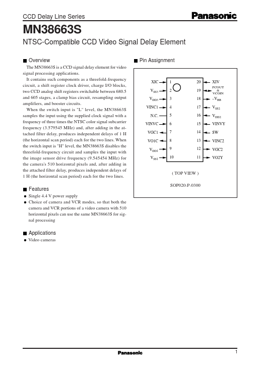
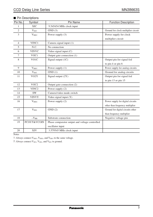
Pin No. VBB PCOUT&VCOIN XIV Pin Name 9.545454 MHz clock input GND (3) Power supply (3) Camera signal input (1) No connection Video signal input (C) Output gate connection (1) Signal output (1C) Power supply (1) GND (1) Signal output (2Y) Output gate connection (2) Power supply (2) Camera/video mode switch Video signal input (Y) Power supply (2)
📁 MN38663S Similar Datasheet