Datasheet Details
| Part number | MN3880S |
|---|---|
| Manufacturer | Panasonic |
| File Size | 43.57 KB |
| Description | NTSC CCD Video Signal Delay Element |
| Datasheet |
 MN3880S Datasheet MN3880S Datasheet
|
|
|
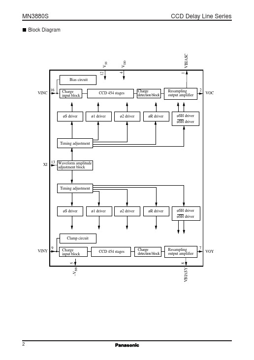
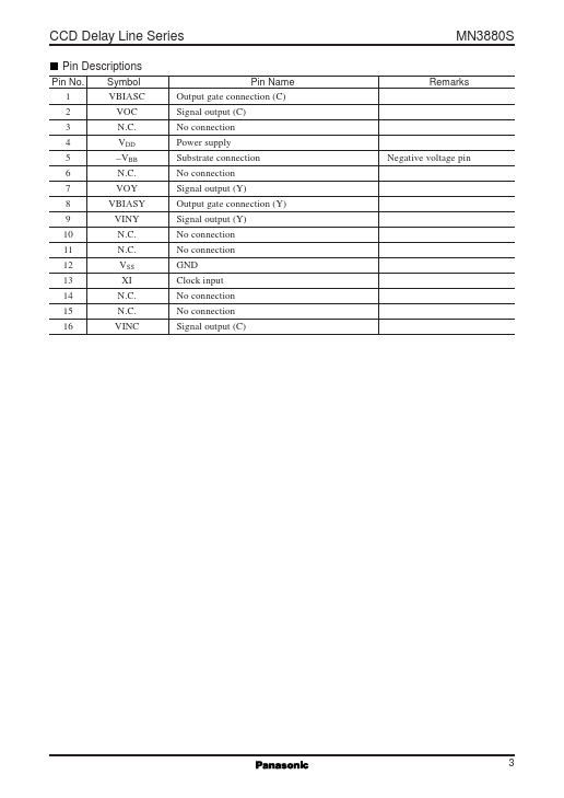
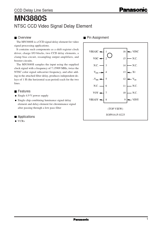
Pin No.
1 2 3 4 5 6 7 8 9 10 11 12 13 14 15 16 Symbol VBIASC VOC N.C.
VBB N.C.
VOY VBIASY VINY N.C.
N.C.
| Part number | MN3880S |
|---|---|
| Manufacturer | Panasonic |
| File Size | 43.57 KB |
| Description | NTSC CCD Video Signal Delay Element |
| Datasheet |
MN3880S Datasheet
|
|
|
|