Datasheet4U Logo Datasheet4U.com

PLL103-05

1-to-5 Clock Distribution Buffer

PLL103-05 Features

* 5 outputs identical to FIN. Low skew (< 250 ps between outputs). Input / Output frequency range 0

* 160 MHz 25mA drive capability at TTL levels. 70mA drive capability at CMOS levels. 3.3V operation. Available in 8-Pin 150m

PLL103-05 General Description

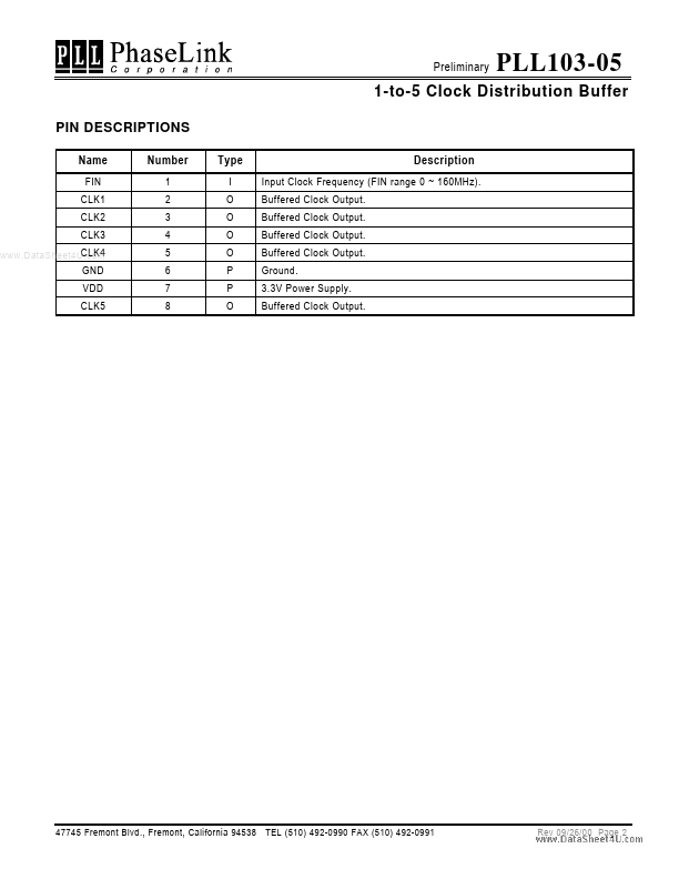
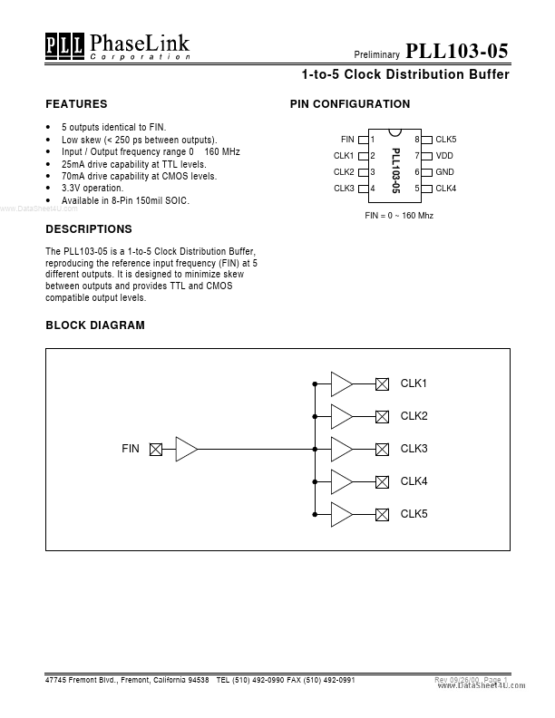
The PLL103-05 is a 1-to-5 Clock Distribution Buffer, reproducing the reference input frequency (FIN) at 5 different outputs. It is designed to minimize skew between outputs and provides TTL and CMOS compatible output levels. BLOCK DIAGRAM CLK1 CLK2 FIN CLK3 CLK4 CLK5 47745 Fremont Blvd., Fremont.

PLL103-05 Datasheet (150.51 KB)

Preview of PLL103-05 PDF

Datasheet Details

Part number:

PLL103-05

Manufacturer:

PhaseLink Corporation

File Size:

150.51 KB

Description:

1-to-5 clock distribution buffer.

📁 Related Datasheet

PLL103-01 Low Skew Buffer (PhaseLink Corporation)

PLL103-02 DDR SDRAM Buffer (PhaseLink Corporation)

PLL103-03 DDR SDRAM Buffer (PhaseLink Corporation)

PLL103-04 1-to-4 Clock Distribution Buffer (PhaseLink Corporation)

PLL103-06 DDR SDRAM Buffer (PhaseLink Corporation)

PLL103-07 2 DIMM DDR Fanout Buffer (PhaseLink Corporation)

PLL103-11 Low Skew Buffers (PhaseLink Corporation)

PLL103-53 DDR SDRAM Buffer (PhaseLink Corporation)

PLL1000A PHASE LOCKED LOOP (Z-Communications)

PLL102-03 Low Skew Output Buffer (PhaseLink Corporation)

TAGS

PLL103-05 1-to-5 Clock Distribution Buffer PhaseLink Corporation

Image Gallery

PLL103-05 Datasheet Preview Page 2 PLL103-05 Datasheet Preview Page 3

PLL103-05 Distributor