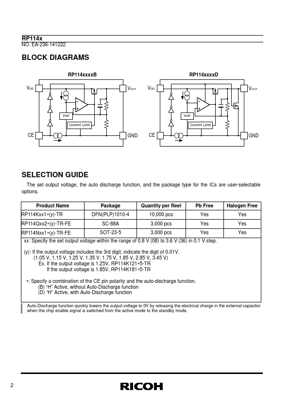
Description
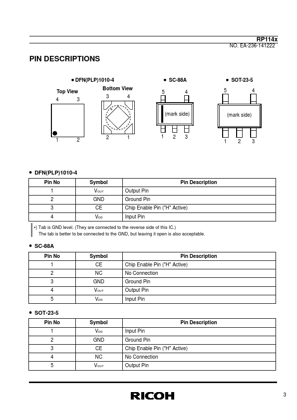
DFN(PLP)1010-4
Top View 43
Bottom View 34
∗
12
21
SC-88A
54
(mark side)
123
RP114x
NO.EA-236-141222
SOT-23-5
54
(mark side)
123
DFN(PLP)1010-4
Pin No 1 2 3 4
Symbol VOUT GND CE VDD
Pin Description Output Pin Ground Pin Chip Enable Pin ("H" Active) Input Pin
∗) Tab is GND level.(They are connected to the reverse side of this IC.) The tab is better to be connected to the GND, but leaving it open is also acceptable.
SC-88A
Pin No 1 2
Features
- a minimum input voltage from 1.4V and the output voltage, which can be set from 0.8V to 3.6V (in 0.1V step). The output voltage of these ICs is internally fixed. These ICs perform with low dropout voltage due to built-in transistor with low ON resistance. Low supply current and a chip enable function prolong the battery life of each system. The ripple rejection, line transient response and load transient response of the RP114x Series are excellent, thus these ICs are very suitable for the power.
 RP114x-RICOHelectronics.pdf