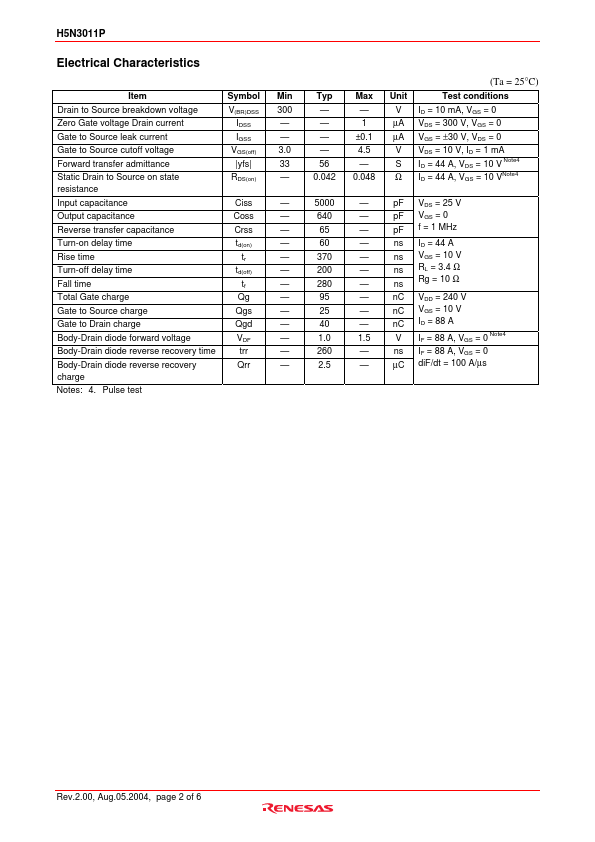
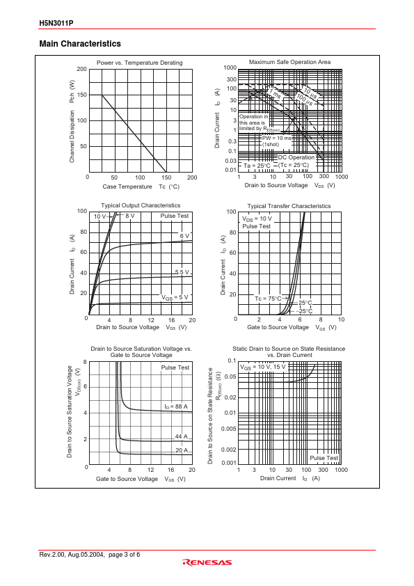
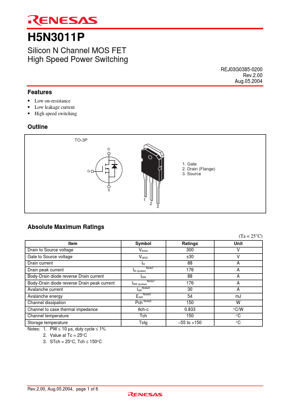
Click to expand full text
H5N3011P
Silicon N Channel MOS FET High Speed Power Switching
Features
• Low on-resistance • Low leakage current • High speed switching
Outline
TO-3P
D
G
S
1 2 3
Absolute Maximum Ratings
Item Drain to Source voltage Gate to Source voltage Drain current Drain peak current Body-Drain diode reverse Drain current Body-Drain diode reverse Drain peak current Avalanche current Avalanche energy Channel dissipation Channel to case thermal impedance Channel temperature Storage temperature Notes: 1. PW ≤ 10 µs, duty cycle ≤ 1%
2. Value at Tc = 25°C 3. STch = 25°C, Tch ≤ 150°C
Symbol
VDSS
VGSS
ID
ID
Note1 (pulse)
IDR
IDR
Note1 (pulse)
IAPNote3
EARNote3
Pch Note2
θch-c
Tch
Tstg
REJ03G0385-0200 Rev.2.00
Aug.05.2004
1. Gate 2. Drain (Flange) 3.
 5N3011P Datasheet