Datasheet Details
| Part number | HD74ALVCH16244 |
|---|---|
| Manufacturer | Renesas |
| File Size | 119.11 KB |
| Description | 16-bit Buffers / Drivers |
| Datasheet |
 HD74ALVCH16244 Datasheet HD74ALVCH16244 Datasheet
|
|
|
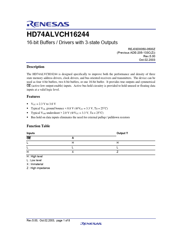
The HD74ALVCH16244 is designed specifically to improve both the performance and density of three state memory address drivers, clock drivers, and bus oriented receivers and transmitters.
The device can be used as four 4-bit buffers, two 8-bit buffers, or one 16-bit buffer.
| Part number | HD74ALVCH16244 |
|---|---|
| Manufacturer | Renesas |
| File Size | 119.11 KB |
| Description | 16-bit Buffers / Drivers |
| Datasheet |
HD74ALVCH16244 Datasheet
|
|
|
|