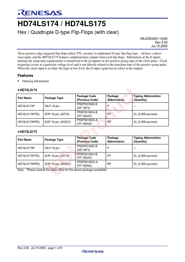
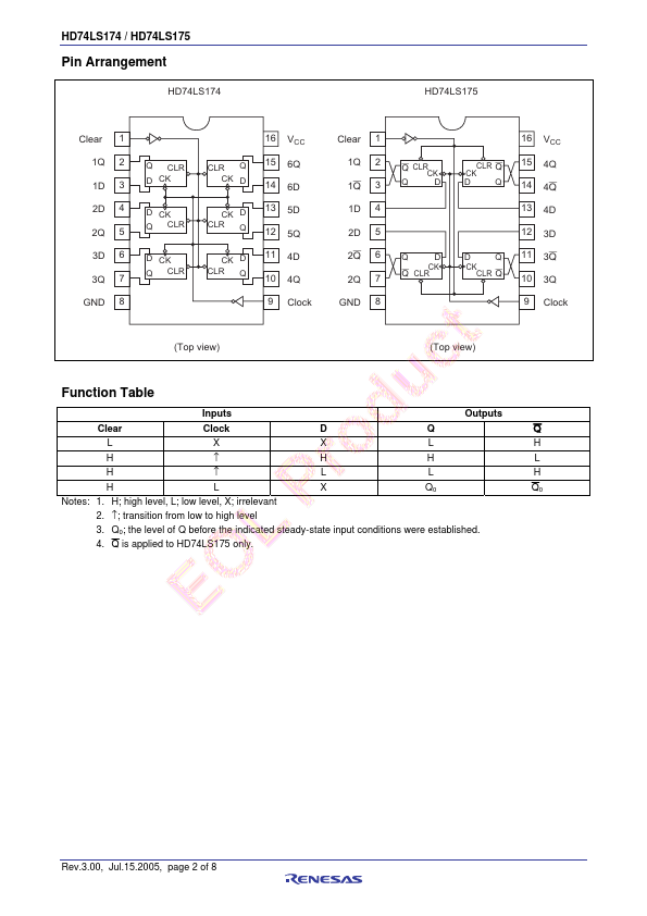
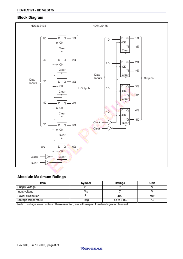
Datasheet4U Logo Datasheet4U.com

HD74LS175P Datasheet - Renesas

Hex / Quadruple D-type Flip-Flops

HD74LS175P Features

* complementary outputs from each flip-flops. Information at the D inputs meeting the setup time requirements is transferred to the Q outputs on the positive-going edge of the clock pulse. Clock triggering occurs at a particular voltage level and is not directly related to the transition time of the p

HD74LS175P Datasheet (243.78 KB)

Preview of HD74LS175P PDF

Datasheet Details

Part number:

HD74LS175P

Manufacturer:

Renesas ↗

File Size:

243.78 KB

Description:

Hex / quadruple d-type flip-flops.
HD74LS174 / HD74LS175 Hex / Quadruple D-type Flip-Flops (with clear) REJ03D0451 0300 Rev.3.00 Jul.15.2005 These positive-edge-triggered fli.

📁 Related Datasheet

HD74LS175 Hex/Quadruple D-type Flip-Flips (Hitachi Semiconductor)

HD74LS175 Hex / Quadruple D-type Flip-Flops (Renesas)

HD74LS170 4-by-4 Register File (Hitachi Semiconductor)

HD74LS174 Hex/Quadruple D-type Flip-Flips (Hitachi Semiconductor)

HD74LS174 Hex / Quadruple D-type Flip-Flops (Renesas)

HD74LS174P Hex / Quadruple D-type Flip-Flops (Renesas)

HD74LS10 Triple 3-input Positive NAND Gates (Hitachi Semiconductor)

HD74LS10 Triple 3-Input Positive NAND Gates (Renesas)

HD74LS107A Dual J-K Negative-edge-triggered Flip-Flops (Hitachi Semiconductor)

HD74LS107A Dual J-K Negative-edge-triggered Flip-Flops (Renesas)

TAGS

HD74LS175P Hex Quadruple D-type Flip-Flops Renesas

Image Gallery

HD74LS175P Datasheet Preview Page 2 HD74LS175P Datasheet Preview Page 3

HD74LS175P Distributor