Datasheet Details
| Part number | M29F512B |
|---|---|
| Manufacturer | STMicroelectronics ↗ |
| File Size | 136.05 KB |
| Description | 512 Kbit 64Kb x8 / Bulk Single Supply Flash Memory |
| Datasheet |
 M29F512B_STMicroelectronics.pdf M29F512B_STMicroelectronics.pdf
|
| Part number | M29F512B |
|---|---|
| Manufacturer | STMicroelectronics ↗ |
| File Size | 136.05 KB |
| Description | 512 Kbit 64Kb x8 / Bulk Single Supply Flash Memory |
| Datasheet |
M29F512B_STMicroelectronics.pdf
|
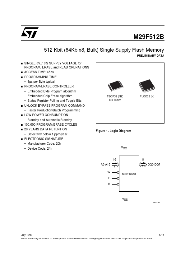
See Figure 1, Logic Diagram, and Table 1, Signal Names, for a brief overview of the signals connected to this device.
📁 M29F512B Similar Datasheet