Description
XDR DRAM
The timing diagrams in Figure 1 illustrate XDR DRAM device write and read transactions.There are three sets of pins used for normal memory access transactions: CFM/CFMN clock pins, RQ11..0 request pins, and DQ15..0/DQN15..0 data pins.The “N” appended to a signal name denotes the complementary signal of a differential pair.A transaction is a collection of packets needed to complete a memory access.A packet is a set of bit windows on the signals of a bus.There are two buses that ca
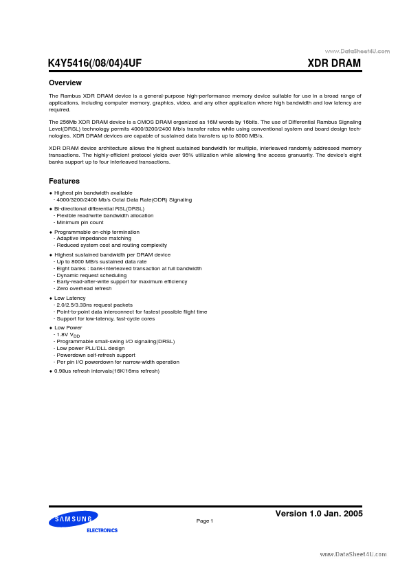
Features
- Highest pin bandwidth available - 4000/3200/2400 Mb/s Octal Data Rate(ODR) Signaling.
- Bi-directional differential RSL(DRSL) - Flexible read/write bandwidth allocation - Minimum pin count.
- Programmable on-chip termination - Adaptive impedance matching - Reduced system cost and routing complexity.
- Highest sustained bandwidth per DRAM device - Up to 8000 MB/s sustained data rate - Eight banks : bank-interleaved transaction at full bandwidth - Dynamic request sch.


