Datasheet4U Logo Datasheet4U.com

K7I161882B, K7I163682B Datasheet - Samsung semiconductor

K7I163682B_Samsungsemiconductor.pdf

This datasheet PDF includes multiple part numbers: K7I161882B, K7I163682B. Please refer to the document for exact specifications by model.
K7I161882B Datasheet Preview Page 2 K7I161882B Datasheet Preview Page 3

Datasheet Details

Part number:

K7I161882B, K7I163682B

Manufacturer:

Samsung semiconductor

File Size:

404.76 KB

Description:

(k7i163682b / k7i161882b) 1mx18-bit ddrii cio b2 sram.

Note:

This datasheet PDF includes multiple part numbers: K7I161882B, K7I163682B.
Please refer to the document for exact specifications by model.

K7I161882B, K7I163682B, (K7I163682B / K7I161882B) 1Mx18-bit DDRII CIO b2 SRAM

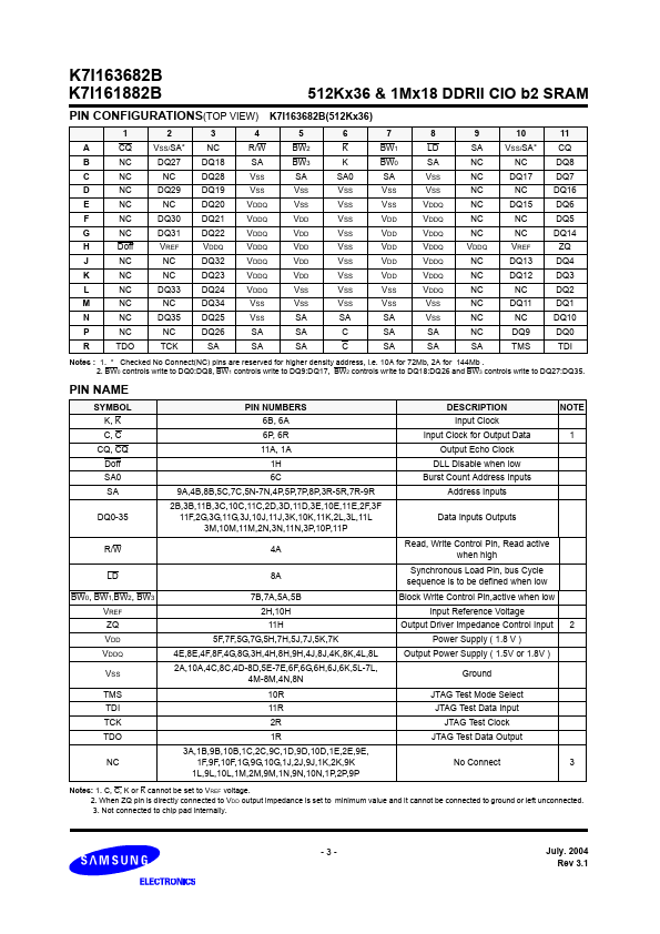
Input Clock Input Clock for Output Data Output Echo Clock DLL Disable when low Burst Count Address Inputs Address Inputs Data Inputs Outputs Read, Write Control Pin, Read active when high Synchronous Load Pin, bus Cycle sequence is to be defined when low Block Write Control Pin,active when low Input

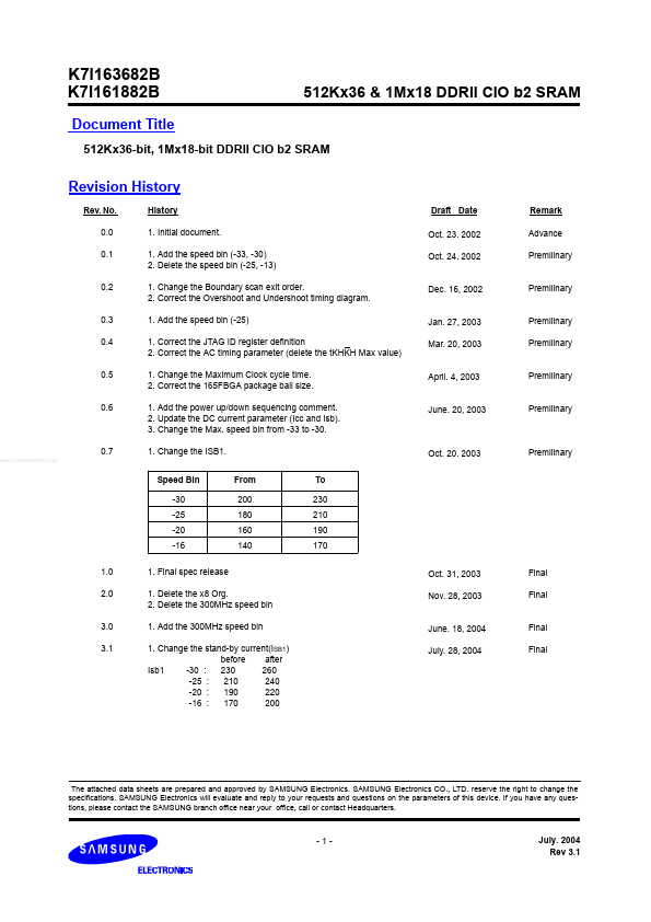
K7I163682B K7I161882B Document Title 512Kx36 & 1Mx18 DDRII CIO b2 SRAM 512Kx36-bit, 1Mx18-bit DDRII CIO b2 SRAM Revision History Rev.

No.

0.0 0.1 History 1.

Initial document.

1.

Add the speed bin (-33, -30) 2.

Delete the speed bin (-25, -13) 1.

Change the Boundary scan exit order.

2.

Correct the Overshoot and Undershoot timing diagram.

1.

Add the speed bin (-25) 1.

Correct the JTAG ID register definition 2.

Correct the AC timing parameter (delete the tKHKH Max value) 1.

Change the Maximum Clo

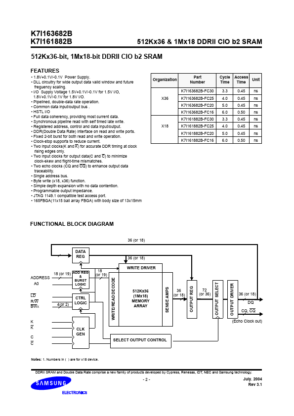
K7I161882B Features

* 1.8V+0.1V/-0.1V Power Supply.

* DLL circuitry for wide output data valid window and future freguency scaling.

* I/O Supply Voltage 1.5V+0.1V/-0.1V for 1.5V I/O, 1.8V+0.1V/-0.1V for 1.8V I/O.

* Pipelined, double-data rate operation.

* Common data input/output

📁 Related Datasheet

📌 All Tags

Samsung semiconductor K7I161882B-like datasheet