Datasheet Details
| Part number | K7I163682B |
|---|---|
| Manufacturer | Samsung semiconductor |
| File Size | 404.76 KB |
| Description | (K7I163682B / K7I161882B) 1Mx18-bit DDRII CIO b2 SRAM |
| Datasheet |
 K7I163682B_Samsungsemiconductor.pdf K7I163682B_Samsungsemiconductor.pdf
|
| Part number | K7I163682B |
|---|---|
| Manufacturer | Samsung semiconductor |
| File Size | 404.76 KB |
| Description | (K7I163682B / K7I161882B) 1Mx18-bit DDRII CIO b2 SRAM |
| Datasheet |
K7I163682B_Samsungsemiconductor.pdf
|
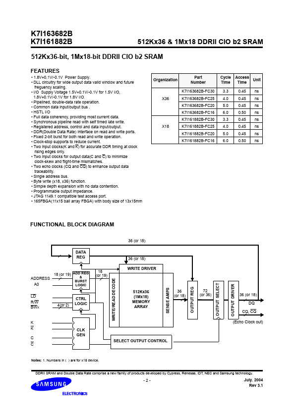
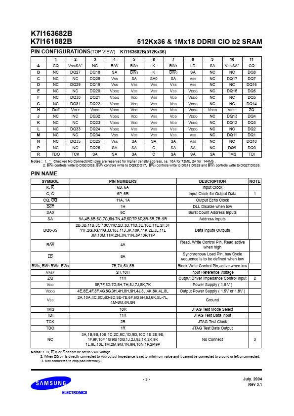
Input Clock Input Clock for Output Data Output Echo Clock DLL Disable when low Burst Count Address Inputs Address Inputs Data Inputs Outputs Read, Write Control Pin, Read active when high Synchronous Load Pin, bus Cycle sequence is to be defined when low Block Write Control Pin,active when low Input Reference Voltage Output Driver Impedance Control Input Power Supply ( 1.8 V ) Output Power Supply ( 1.5V or 1.8V ) Ground JTAG Test Mode Select JTAG Test Data Input JTAG Test Clock JTAG Test Data Ou
📁 K7I163682B Similar Datasheet