Datasheet Details
| Part number | K7I321882M |
|---|---|
| Manufacturer | Samsung semiconductor |
| File Size | 270.13 KB |
| Description | 1Mx36 & 2Mx18 DDRII CIO b2 SRAM |
| Datasheet |
 K7I321882M_Samsungsemiconductor.pdf K7I321882M_Samsungsemiconductor.pdf
|
| Part number | K7I321882M |
|---|---|
| Manufacturer | Samsung semiconductor |
| File Size | 270.13 KB |
| Description | 1Mx36 & 2Mx18 DDRII CIO b2 SRAM |
| Datasheet |
K7I321882M_Samsungsemiconductor.pdf
|
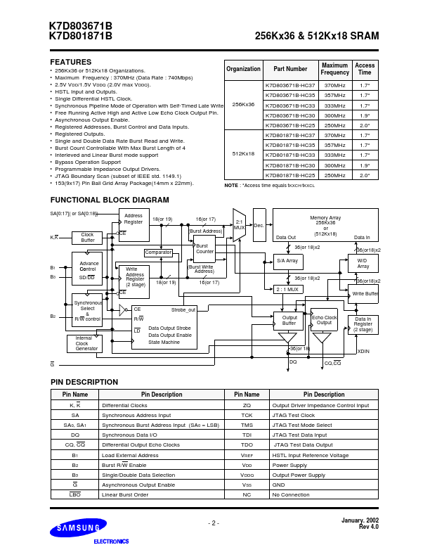
Pin Name K, K SA SA0, SA1 DQ CQ, CQ B1 B2 B3 G LBO Pin Description Differential Clocks Synchronous Address Input Synchronous Burst Address Input (SA 0 = LSB) Synchronous Data I/O Differential Output Echo Clocks Load External Address Burst R/W Enable Single/Double Data Selection Asynchronous Output Enable Linear Burst Order Pin Name ZQ TCK TMS TDI TDO VREF VDD VDDQ VSS NC Pin Description Output Driver Impedance Control Input JTAG Test Clock JTAG Test Mode Select JTAG Test Data Input JTAG Test Dat
📁 K7I321882M Similar Datasheet